
Homework Answers

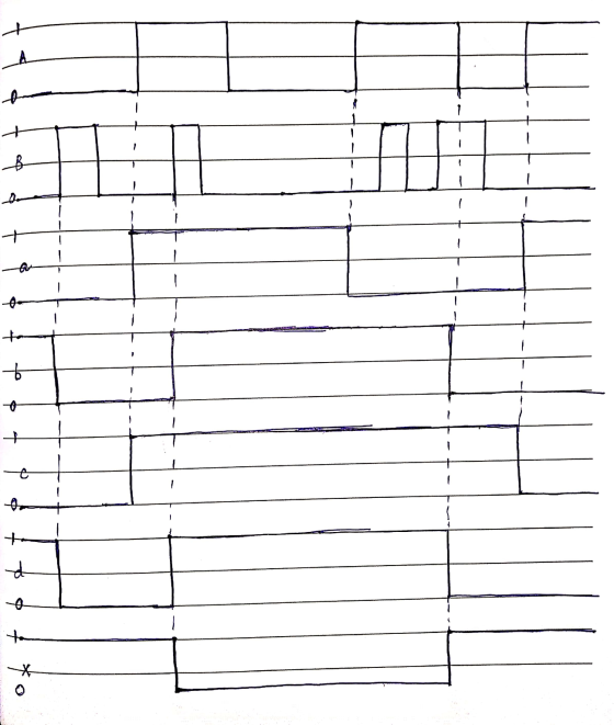
From the given figure, clock pulse and T input to both the T flip flops are the same. Hence when T=1 then clk=1 and whrn T=0 then clk=0. For D flip flop, output follows the truth table only when the clock input is 1. Hence for both D flip flops, output changes as per the truth table only when B=1. Now the timing diagram is as shown below.
(b) Complete the timing diagram for the following circuit. Note that the Ck inputs on the...
 (b) Complete the timing diagram for the following circuit. Note that the Ck inputs on the two flip-flops are different. ClrN Q. Clock 9í CIEN CLR Ck Q||||Q5 || LDCLR D|| Ck Clock O OOON D2 Clock
Complete the timing diagram of Fig. P4.14b by drawing the waveforms of signals 4.14 The circuit...
 Complete the timing diagram of Fig. P4.14b by drawing the
waveforms of signals
4.14 The circuit of Fig. P4.14a contains a D latch, a positive-edge-triggered D flip-flop, and a negative-edge-triggered D flip-flop. Complete the timing diagram of Fig. P4.14b by drawing the waveforms of signals,, and y FI D O Clack Clock Figure P4.14: a. Logic diagram. B. Timing diagram.
Complete the timing diagram of Fig. P4.14b by drawing the
waveforms of signals
4.14 The circuit of Fig. P4.14a contains a D latch, a positive-edge-triggered D flip-flop, and a negative-edge-triggered D flip-flop. Complete the timing diagram of Fig. P4.14b by drawing the waveforms of signals,, and y FI D O Clack Clock Figure P4.14: a. Logic diagram. B. Timing diagram.
*) Complete the following timing diagram: b) Complete the following timing diagram: DO Dff clr 7...
 *) Complete the following timing diagram: b) Complete the following timing diagram: DO Dff clr 7 c) Complete the following timing diagram load inp Out clk cir ? cik_unnnnnnnnnnnnn load inp nld Out d) What is this?
For the following sequential circuit, complete the timing diagram and clearly indicate the level changes at...
 For the following sequential circuit, complete the timing
diagram and clearly indicate the level changes at every clock
transition.
Q1 2 Qi Q ?? Q2 Q2 D2 CK Clr CK Kl Clock Clr OC X-J1 Q1 D2
For the following sequential circuit, complete the timing
diagram and clearly indicate the level changes at every clock
transition.
Q1 2 Qi Q ?? Q2 Q2 D2 CK Clr CK Kl Clock Clr OC X-J1 Q1 D2
PROBLEM 2 (83 PTS) Complete the timing diagram of the circuit shown below: (10 pts) Full...
 PROBLEM 2 (83 PTS) Complete the timing diagram of the circuit shown below: (10 pts) Full Adder clk resetn cin cout Cout clk resetn cout I Complete the timing diagram of the circuit shown below: (7 pts) resetn clk resetn clk
PROBLEM 1 (12 PTS) Complete the timing diagram of the circuit shown below. (5 pts) resetn...
 PROBLEM 1 (12 PTS) Complete the timing diagram of the circuit shown below. (5 pts) resetn clock resetn clock Complete the timing diagram of the circuits shown below: (7 pts) · reset clk resetn Latch
Complete the timing diagram of the following circuit. G = G-G2G,Go-1011, Q Q3QaQ1Qo resetn clk clk...
 Complete the timing diagram of the following circuit. G = G-G2G,Go-1011, Q Q3QaQ1Qo resetn clk clk resetn Q 0000 | ﹁ ㄒㄧ | ﹁ ㄒㄧ | ㄒㄧ | ㄒㄧ |-
Q8 Complete the timing diagram of the circuit in Fig. A8. Signal 002 TOD top Clock...
 Q8 Complete the timing diagram of the circuit in Fig. A8. Signal 002 TOD top Clock Fig. A8 Clock
Complete the timing diagram for the given circuit. Assume that both gates have a propagation delay...
 Complete the timing diagram for the given circuit.
Assume that both gates have a propagation delay of 8
ns.
DD 0 5 10 15 20 25 30 35 40 t(ns)
Complete the timing diagram for the given circuit.
Assume that both gates have a propagation delay of 8
ns.
DD 0 5 10 15 20 25 30 35 40 t(ns)
Question 10 (5 marks) A combinational logic circuit is shown in Figure 3 along with a timing diagram. a) The output waveform (X) shown in the timing diagram is not correct for the circuit shown....
 Question 10 (5 marks) A combinational logic circuit is shown in Figure 3 along with a timing diagram. a) The output waveform (X) shown in the timing diagram is not correct for the circuit shown. Draw the correct waveform. (2 marks) b) The output waveform shown is the result of incorrect implementation of the circuit gates has been replaced by another type of gate. Which gate has been replaced and what is the replacement gate? Explain your answer. (3 marks)...
 (b) Complete the timing diagram for the following circuit. Note that the Ck inputs on the two flip-flops are different. ClrN Q. Clock 9í CIEN CLR Ck Q||||Q5 || LDCLR D|| Ck Clock O OOON D2 Clock
 Complete the timing diagram of Fig. P4.14b by drawing the
waveforms of signals
4.14 The circuit of Fig. P4.14a contains a D latch, a positive-edge-triggered D flip-flop, and a negative-edge-triggered D flip-flop. Complete the timing diagram of Fig. P4.14b by drawing the waveforms of signals,, and y FI D O Clack Clock Figure P4.14: a. Logic diagram. B. Timing diagram.
Complete the timing diagram of Fig. P4.14b by drawing the
waveforms of signals
4.14 The circuit of Fig. P4.14a contains a D latch, a positive-edge-triggered D flip-flop, and a negative-edge-triggered D flip-flop. Complete the timing diagram of Fig. P4.14b by drawing the waveforms of signals,, and y FI D O Clack Clock Figure P4.14: a. Logic diagram. B. Timing diagram.
 *) Complete the following timing diagram: b) Complete the following timing diagram: DO Dff clr 7 c) Complete the following timing diagram load inp Out clk cir ? cik_unnnnnnnnnnnnn load inp nld Out d) What is this?
 For the following sequential circuit, complete the timing
diagram and clearly indicate the level changes at every clock
transition.
Q1 2 Qi Q ?? Q2 Q2 D2 CK Clr CK Kl Clock Clr OC X-J1 Q1 D2
For the following sequential circuit, complete the timing
diagram and clearly indicate the level changes at every clock
transition.
Q1 2 Qi Q ?? Q2 Q2 D2 CK Clr CK Kl Clock Clr OC X-J1 Q1 D2
 PROBLEM 2 (83 PTS) Complete the timing diagram of the circuit shown below: (10 pts) Full Adder clk resetn cin cout Cout clk resetn cout I Complete the timing diagram of the circuit shown below: (7 pts) resetn clk resetn clk
 PROBLEM 1 (12 PTS) Complete the timing diagram of the circuit shown below. (5 pts) resetn clock resetn clock Complete the timing diagram of the circuits shown below: (7 pts) · reset clk resetn Latch
 Complete the timing diagram of the following circuit. G = G-G2G,Go-1011, Q Q3QaQ1Qo resetn clk clk resetn Q 0000 | ﹁ ㄒㄧ | ﹁ ㄒㄧ | ㄒㄧ | ㄒㄧ |-
 Q8 Complete the timing diagram of the circuit in Fig. A8. Signal 002 TOD top Clock Fig. A8 Clock
 Complete the timing diagram for the given circuit.
Assume that both gates have a propagation delay of 8
ns.
DD 0 5 10 15 20 25 30 35 40 t(ns)
Complete the timing diagram for the given circuit.
Assume that both gates have a propagation delay of 8
ns.
DD 0 5 10 15 20 25 30 35 40 t(ns)
 Question 10 (5 marks) A combinational logic circuit is shown in Figure 3 along with a timing diagram. a) The output waveform (X) shown in the timing diagram is not correct for the circuit shown. Draw the correct waveform. (2 marks) b) The output waveform shown is the result of incorrect implementation of the circuit gates has been replaced by another type of gate. Which gate has been replaced and what is the replacement gate? Explain your answer. (3 marks)...
Most questions answered within 3 hours.
-
Where is the error in this code sequence?
String s1 = "Hello";
String s2 = "ello";...
asked 10 months ago -
Financial data for Joel de Paris, Inc., for last year
follow:
Joel de Paris, Inc.
Balance...
asked 10 months ago -
Consider this reaction:
Al2(SO4)3 (aq)+ BaCl3
(aq) Al2Cl6 (aq)- +
3BaSO4(s) . What is the...
asked 10 months ago -
Suppose that Savneet is considering increasing her
recent random sample from 20 car rentals to 40...
asked 10 months ago -
Trucks arrive at an unloading terminal at an average rate of 120
per hour.
Trucks arrive...
asked 10 months ago -
Why are methanol and ethanol completely soluble in water while
octanol is not very little soluble....
asked 10 months ago -
A facilities manager at a university reads in a research report
that the mean amount of...
asked 10 months ago -
When the CuSO4 is rehydrated by adding water to the anhydrous
compound, is this an endothermic...
asked 10 months ago -
A ray of sunlight is passing from diamond into crown glass; the
angle of incidence is...
asked 10 months ago -
A block of mass 0.249 kg is placed on top of a light, vertical
spring of...
asked 10 months ago -
how do the kidneys compensate in the presences of acidosis
a) trigger hyperventilate
b) reserve acid...
asked 10 months ago -
Question 501 pts
The rental rate of capital to the firm increases. Which of the
following...
asked 10 months ago