
Homework Answers
Dear student, the detailed solution is shown below. If you have any queries regarding the solution please comment. If you find the answer helpful please rate it.

Thanks!
Add Answer to:
please show calculations
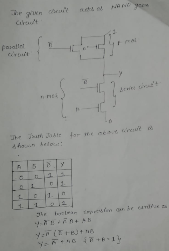
Consider the following circuit of pMOS and nMOS transistors. B-[ A6 AC What...
The layout of a CMOS complex logic circuit is given in the Figure 1 4. Draw the corresponding circuit diagram; and (10 Marks) a. b. Calculate the (W) of all the nMOS and PMOS transistors for simul...
 The layout of a CMOS complex logic circuit is given in the Figure 1 4. Draw the corresponding circuit diagram; and (10 Marks) a. b. Calculate the (W) of all the nMOS and PMOS transistors for simultaneous switching (W/), 15 for all of all the inputs, assuming that (Wh),-20 for all pMOS transistors and (w/L), = 15 for all (WL 20 for all pMOS transistors and (10 Marks) nMOS transistors VDD n well metal poly silicon n+ diffussion OUT Contact...
The layout of a CMOS complex logic circuit is given in the Figure 1. 4. Draw the corresponding circuit diagram; and (10 Marks) a. b. Colculate the W/Doivalent of all the nMOS and PMOS transistors...
 The layout of a CMOS complex logic circuit is given in the Figure 1. 4. Draw the corresponding circuit diagram; and (10 Marks) a. b. Colculate the W/Doivalent of all the nMOS and PMOS transistors for simultaneous switching of all the inputs, assuming that (W/, 25 for all MOS transistors and (W/, 20 for al nMOS transistors. (10 Marks) FIA, B,C,D,E ) A B Figure 1
The layout of a CMOS complex logic circuit is given in the Figure 1....
The layout of a CMOS complex logic circuit is given in the Figure 1. 4. Draw the corresponding circuit diagram; and (10 Marks) a. b. Colculate the W/Doivalent of all the nMOS and PMOS transistors for simultaneous switching of all the inputs, assuming that (W/, 25 for all MOS transistors and (W/, 20 for al nMOS transistors. (10 Marks) FIA, B,C,D,E ) A B Figure 1
The layout of a CMOS complex logic circuit is given in the Figure 1....
with details and explanations 4. The layout of a CMOS complex logic circuit is eiven in the Figure 1 (10 Marks) Calculate the (/equvalent of all the nMoS and PMOS transistors for simultaneous swit...
 with details and explanations
4. The layout of a CMOS complex logic circuit is eiven in the Figure 1 (10 Marks) Calculate the (/equvalent of all the nMoS and PMOS transistors for simultaneous switching of all the inputs, assuming that (W/1), 15 for all pMOS transistors and (W/L), 5 for all nMOS Draw the corresponding circuit diagram; and a. b. (10 Marks) transistors Vdd PMOS NMOS GND Figure 1
4. The layout of a CMOS complex logic circuit is eiven...
with details and explanations
4. The layout of a CMOS complex logic circuit is eiven in the Figure 1 (10 Marks) Calculate the (/equvalent of all the nMoS and PMOS transistors for simultaneous switching of all the inputs, assuming that (W/1), 15 for all pMOS transistors and (W/L), 5 for all nMOS Draw the corresponding circuit diagram; and a. b. (10 Marks) transistors Vdd PMOS NMOS GND Figure 1
4. The layout of a CMOS complex logic circuit is eiven...
The layout of a CMOS complex logiccircuit is given in the Figure 1 4. (10 Marks) a. Draw the corresponding circuit diagram;and b. calculate the (uivains f allthe nMoS and PMOS transistors for simulta...
 The layout of a CMOS complex logiccircuit is given in the Figure 1 4. (10 Marks) a. Draw the corresponding circuit diagram;and b. calculate the (uivains f allthe nMoS and PMOS transistors for simultaneous switching of all the inputs, assumingthat(W/15 for all pMOS transistors and 10 for all equivalent 15 for all pMOS transistors and(W/D)10for all (10 Marks) nMOS transistors. n+ diffusion p+ diffusion ■ metal OUT polysilicon GND Figure 1
The layout of a CMOS complex logiccircuit is given...
The layout of a CMOS complex logiccircuit is given in the Figure 1 4. (10 Marks) a. Draw the corresponding circuit diagram;and b. calculate the (uivains f allthe nMoS and PMOS transistors for simultaneous switching of all the inputs, assumingthat(W/15 for all pMOS transistors and 10 for all equivalent 15 for all pMOS transistors and(W/D)10for all (10 Marks) nMOS transistors. n+ diffusion p+ diffusion ■ metal OUT polysilicon GND Figure 1
The layout of a CMOS complex logiccircuit is given...
4. The layout of a CMOS complex logic circuit is given in the Figure t n A to l nd D using (10 Marks) qulatent of all the nmos and PMos transistors for simultaneous switching of for atl noS a. Dra...
 4. The layout of a CMOS complex logic circuit is given in the Figure t n A to l nd D using (10 Marks) qulatent of all the nmos and PMos transistors for simultaneous switching of for atl noS a. Draw the corresponding circuit diagram; and b. Calculate the (WI/n cqutvatent Of l all the inputs, assuming that (/) 15 for all pMOS transistors and (W/)- a viron ne, (10 Marks) transistors and -Vdd rol pMOS NMOS s GND
4....
4. The layout of a CMOS complex logic circuit is given in the Figure t n A to l nd D using (10 Marks) qulatent of all the nmos and PMos transistors for simultaneous switching of for atl noS a. Draw the corresponding circuit diagram; and b. Calculate the (WI/n cqutvatent Of l all the inputs, assuming that (/) 15 for all pMOS transistors and (W/)- a viron ne, (10 Marks) transistors and -Vdd rol pMOS NMOS s GND
4....
5. The NMOS and PMOS transistors in the below circuit are matched with kn’(Wn/Ln)=kp'(Wp/Lp)=1 mA/V2 and...
 5. The NMOS and PMOS transistors in the below circuit are matched with kn’(Wn/Ln)=kp'(Wp/Lp)=1 mA/V2 and Vin=-Vt=1V. (20 pts) +5 V a) Which MOSFET is cut-off, NMOS (QN) or PMOS (QP) for VF-5V? Why (5 pts) Qp -5 Vo Ipp Vo VION ON -5 V b) When VF-5V, in which mode, saturation or triode, the circuit operate? Explain why? (5 pts) c) Find the drain current ipy and ipp and the voltage vo for VF-5V (10 pts)
Prob 2. Implement the logic function Y = (Ā + B)D in static CMOS. a) Size the transistors so that the output resistance is the same as that of a an nMOS (W/L-0.4/0.18) and pMOS (W/L-0.8/0.18). b)...
 Prob 2. Implement the logic function Y = (Ā + B)D in static CMOS. a) Size the transistors so that the output resistance is the same as that of a an nMOS (W/L-0.4/0.18) and pMOS (W/L-0.8/0.18). b) What input combination(s) result in the worst case tpiti.? c) Determine the worst case tpl for a 100 iF load capacitance. Use equivalent resistance model, Req
Prob 2. Implement the logic function Y = (Ā + B)D in static CMOS. a) Size the...
Prob 2. Implement the logic function Y = (Ā + B)D in static CMOS. a) Size the transistors so that the output resistance is the same as that of a an nMOS (W/L-0.4/0.18) and pMOS (W/L-0.8/0.18). b) What input combination(s) result in the worst case tpiti.? c) Determine the worst case tpl for a 100 iF load capacitance. Use equivalent resistance model, Req
Prob 2. Implement the logic function Y = (Ā + B)D in static CMOS. a) Size the...
with details and explanations 3. Consider the logic function Z-((A + B).D). (C.(E+F)) (5 Marks) Realize the above Boolean function using CMOS transistors. a. btain a common Euler path for both nMO...
 with details and explanations
3. Consider the logic function Z-((A + B).D). (C.(E+F)) (5 Marks) Realize the above Boolean function using CMOS transistors. a. btain a common Euler path for both nMOS and pMOS transistors and hence draw the optimized stick diagram layout. b. O (30 Marks)
3. Consider the logic function Z-((A + B).D). (C.(E+F)) (5 Marks) Realize the above Boolean function using CMOS transistors. a. btain a common Euler path for both nMOS and pMOS transistors and hence...
with details and explanations
3. Consider the logic function Z-((A + B).D). (C.(E+F)) (5 Marks) Realize the above Boolean function using CMOS transistors. a. btain a common Euler path for both nMOS and pMOS transistors and hence draw the optimized stick diagram layout. b. O (30 Marks)
3. Consider the logic function Z-((A + B).D). (C.(E+F)) (5 Marks) Realize the above Boolean function using CMOS transistors. a. btain a common Euler path for both nMOS and pMOS transistors and hence...
CMOS Design Styles Quiz Problem 1: a) What is the typical "topology" for pMOS and nMOS...
CMOS Design Styles Quiz Problem 1: a) What is the typical "topology" for pMOS and nMOS in digital circuitry? -pMOS Vdd to Vout, nMOS Vout to Gnd -nMOS Vdd to Vout, pMOS Vout to Gnd -pMOS Vdd to Gnd, nMOS Vin to Vout -Only use xMOS -Both transistors Vin to Vout b) How do you implement nMOS in AND functions? -series connected, with increased widths -Parallel connected, with standard widths -Series connected with half the widths -Parallel connected, alternating large...
Using PMOS and NMOS construct a fall adder circuit. What are the best cases and worst cases for b...
Using PMOS and NMOS construct a fall adder circuit. What are the best cases and worst cases for both rise time delay (Tdr) and fall time delay (Tdf)?
 The layout of a CMOS complex logic circuit is given in the Figure 1 4. Draw the corresponding circuit diagram; and (10 Marks) a. b. Calculate the (W) of all the nMOS and PMOS transistors for simultaneous switching (W/), 15 for all of all the inputs, assuming that (Wh),-20 for all pMOS transistors and (w/L), = 15 for all (WL 20 for all pMOS transistors and (10 Marks) nMOS transistors VDD n well metal poly silicon n+ diffussion OUT Contact...
 The layout of a CMOS complex logic circuit is given in the Figure 1. 4. Draw the corresponding circuit diagram; and (10 Marks) a. b. Colculate the W/Doivalent of all the nMOS and PMOS transistors for simultaneous switching of all the inputs, assuming that (W/, 25 for all MOS transistors and (W/, 20 for al nMOS transistors. (10 Marks) FIA, B,C,D,E ) A B Figure 1
The layout of a CMOS complex logic circuit is given in the Figure 1....
The layout of a CMOS complex logic circuit is given in the Figure 1. 4. Draw the corresponding circuit diagram; and (10 Marks) a. b. Colculate the W/Doivalent of all the nMOS and PMOS transistors for simultaneous switching of all the inputs, assuming that (W/, 25 for all MOS transistors and (W/, 20 for al nMOS transistors. (10 Marks) FIA, B,C,D,E ) A B Figure 1
The layout of a CMOS complex logic circuit is given in the Figure 1....
 with details and explanations
4. The layout of a CMOS complex logic circuit is eiven in the Figure 1 (10 Marks) Calculate the (/equvalent of all the nMoS and PMOS transistors for simultaneous switching of all the inputs, assuming that (W/1), 15 for all pMOS transistors and (W/L), 5 for all nMOS Draw the corresponding circuit diagram; and a. b. (10 Marks) transistors Vdd PMOS NMOS GND Figure 1
4. The layout of a CMOS complex logic circuit is eiven...
with details and explanations
4. The layout of a CMOS complex logic circuit is eiven in the Figure 1 (10 Marks) Calculate the (/equvalent of all the nMoS and PMOS transistors for simultaneous switching of all the inputs, assuming that (W/1), 15 for all pMOS transistors and (W/L), 5 for all nMOS Draw the corresponding circuit diagram; and a. b. (10 Marks) transistors Vdd PMOS NMOS GND Figure 1
4. The layout of a CMOS complex logic circuit is eiven...
 The layout of a CMOS complex logiccircuit is given in the Figure 1 4. (10 Marks) a. Draw the corresponding circuit diagram;and b. calculate the (uivains f allthe nMoS and PMOS transistors for simultaneous switching of all the inputs, assumingthat(W/15 for all pMOS transistors and 10 for all equivalent 15 for all pMOS transistors and(W/D)10for all (10 Marks) nMOS transistors. n+ diffusion p+ diffusion ■ metal OUT polysilicon GND Figure 1
The layout of a CMOS complex logiccircuit is given...
The layout of a CMOS complex logiccircuit is given in the Figure 1 4. (10 Marks) a. Draw the corresponding circuit diagram;and b. calculate the (uivains f allthe nMoS and PMOS transistors for simultaneous switching of all the inputs, assumingthat(W/15 for all pMOS transistors and 10 for all equivalent 15 for all pMOS transistors and(W/D)10for all (10 Marks) nMOS transistors. n+ diffusion p+ diffusion ■ metal OUT polysilicon GND Figure 1
The layout of a CMOS complex logiccircuit is given...
 4. The layout of a CMOS complex logic circuit is given in the Figure t n A to l nd D using (10 Marks) qulatent of all the nmos and PMos transistors for simultaneous switching of for atl noS a. Draw the corresponding circuit diagram; and b. Calculate the (WI/n cqutvatent Of l all the inputs, assuming that (/) 15 for all pMOS transistors and (W/)- a viron ne, (10 Marks) transistors and -Vdd rol pMOS NMOS s GND
4....
4. The layout of a CMOS complex logic circuit is given in the Figure t n A to l nd D using (10 Marks) qulatent of all the nmos and PMos transistors for simultaneous switching of for atl noS a. Draw the corresponding circuit diagram; and b. Calculate the (WI/n cqutvatent Of l all the inputs, assuming that (/) 15 for all pMOS transistors and (W/)- a viron ne, (10 Marks) transistors and -Vdd rol pMOS NMOS s GND
4....
 5. The NMOS and PMOS transistors in the below circuit are matched with kn’(Wn/Ln)=kp'(Wp/Lp)=1 mA/V2 and Vin=-Vt=1V. (20 pts) +5 V a) Which MOSFET is cut-off, NMOS (QN) or PMOS (QP) for VF-5V? Why (5 pts) Qp -5 Vo Ipp Vo VION ON -5 V b) When VF-5V, in which mode, saturation or triode, the circuit operate? Explain why? (5 pts) c) Find the drain current ipy and ipp and the voltage vo for VF-5V (10 pts)
 Prob 2. Implement the logic function Y = (Ā + B)D in static CMOS. a) Size the transistors so that the output resistance is the same as that of a an nMOS (W/L-0.4/0.18) and pMOS (W/L-0.8/0.18). b) What input combination(s) result in the worst case tpiti.? c) Determine the worst case tpl for a 100 iF load capacitance. Use equivalent resistance model, Req
Prob 2. Implement the logic function Y = (Ā + B)D in static CMOS. a) Size the...
Prob 2. Implement the logic function Y = (Ā + B)D in static CMOS. a) Size the transistors so that the output resistance is the same as that of a an nMOS (W/L-0.4/0.18) and pMOS (W/L-0.8/0.18). b) What input combination(s) result in the worst case tpiti.? c) Determine the worst case tpl for a 100 iF load capacitance. Use equivalent resistance model, Req
Prob 2. Implement the logic function Y = (Ā + B)D in static CMOS. a) Size the...
 with details and explanations
3. Consider the logic function Z-((A + B).D). (C.(E+F)) (5 Marks) Realize the above Boolean function using CMOS transistors. a. btain a common Euler path for both nMOS and pMOS transistors and hence draw the optimized stick diagram layout. b. O (30 Marks)
3. Consider the logic function Z-((A + B).D). (C.(E+F)) (5 Marks) Realize the above Boolean function using CMOS transistors. a. btain a common Euler path for both nMOS and pMOS transistors and hence...
with details and explanations
3. Consider the logic function Z-((A + B).D). (C.(E+F)) (5 Marks) Realize the above Boolean function using CMOS transistors. a. btain a common Euler path for both nMOS and pMOS transistors and hence draw the optimized stick diagram layout. b. O (30 Marks)
3. Consider the logic function Z-((A + B).D). (C.(E+F)) (5 Marks) Realize the above Boolean function using CMOS transistors. a. btain a common Euler path for both nMOS and pMOS transistors and hence...
Most questions answered within 3 hours.
-
Where is the error in this code sequence?
String s1 = "Hello";
String s2 = "ello";...
asked 10 months ago -
Financial data for Joel de Paris, Inc., for last year
follow:
Joel de Paris, Inc.
Balance...
asked 10 months ago -
Consider this reaction:
Al2(SO4)3 (aq)+ BaCl3
(aq) Al2Cl6 (aq)- +
3BaSO4(s) . What is the...
asked 10 months ago -
Suppose that Savneet is considering increasing her
recent random sample from 20 car rentals to 40...
asked 10 months ago -
Trucks arrive at an unloading terminal at an average rate of 120
per hour.
Trucks arrive...
asked 10 months ago -
Why are methanol and ethanol completely soluble in water while
octanol is not very little soluble....
asked 10 months ago -
A facilities manager at a university reads in a research report
that the mean amount of...
asked 10 months ago -
When the CuSO4 is rehydrated by adding water to the anhydrous
compound, is this an endothermic...
asked 10 months ago -
A ray of sunlight is passing from diamond into crown glass; the
angle of incidence is...
asked 10 months ago -
A block of mass 0.249 kg is placed on top of a light, vertical
spring of...
asked 10 months ago -
how do the kidneys compensate in the presences of acidosis
a) trigger hyperventilate
b) reserve acid...
asked 10 months ago -
Question 501 pts
The rental rate of capital to the firm increases. Which of the
following...
asked 10 months ago