
Homework Answers

Add Answer to:
please solve all parts of the question
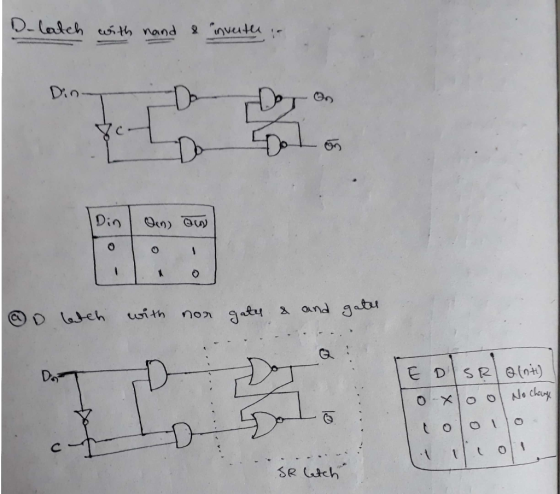
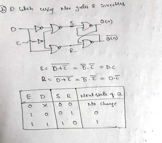
Problem #1 The D latch is constructed with four...
9. (15 points) The D latch shown in lecture 15 slide 15 is constructed with four NAND gates and a...
 9. (15 points) The D latch shown in lecture 15 slide 15 is constructed with four NAND gates and an inverter. Consider the following three other ways for obtaining a D latch, and in each case draw the logic diagram and verify the circuit operation Use NOR gates for the SR latch part and AND gates for the other two. An inverter may be needed. Use NOR gates for all four gates. Inverters may be needed. i. ii. Use four...
a) Draw SR latch impeltation in NOR gates provied function table b) Show how D latch...
a) Draw SR latch impeltation in NOR gates provied function table b) Show how D latch (transprent) can be made from NOR gate. SR latch is transprent when it comes to storing data. c) What is limitation of D latch in terms of storing data ? what does it achive for digital terms d) Design a D flip flop that is -ve edge trigged using master slave combination of D latches designed in b) Inverters may be needed.
CMOS Design Styles Quiz Problem 1: a) What is the typical "topology" for pMOS and nMOS...
CMOS Design Styles Quiz Problem 1: a) What is the typical "topology" for pMOS and nMOS in digital circuitry? -pMOS Vdd to Vout, nMOS Vout to Gnd -nMOS Vdd to Vout, pMOS Vout to Gnd -pMOS Vdd to Gnd, nMOS Vin to Vout -Only use xMOS -Both transistors Vin to Vout b) How do you implement nMOS in AND functions? -series connected, with increased widths -Parallel connected, with standard widths -Series connected with half the widths -Parallel connected, alternating large...
just put circle around the correct answer Chapter 3 Introduction to Logic Gates Questions 1. How...
 just put circle around the correct answer
Chapter 3 Introduction to Logic Gates Questions 1. How many 2-input AND gate required to construct a 5-input AND gate? a) 2 b) 3 d) 4 c) 5 e) noпe Which is better for a 4-input OR gate. The connection of A or B, Fig(13), why? 2. a) A b) B 3. If only 2-input OR gates are available, what is minimum gate level possible to implement an 8-input OR gate 2 a)...
just put circle around the correct answer
Chapter 3 Introduction to Logic Gates Questions 1. How many 2-input AND gate required to construct a 5-input AND gate? a) 2 b) 3 d) 4 c) 5 e) noпe Which is better for a 4-input OR gate. The connection of A or B, Fig(13), why? 2. a) A b) B 3. If only 2-input OR gates are available, what is minimum gate level possible to implement an 8-input OR gate 2 a)...
1.) In a CMOS NAND gate, if only one PMOS is ON, the output is low...
1.) In a CMOS NAND gate, if only one PMOS is ON, the output is low voltage (logic 0) High voltage (logic high) depends on the state of NMOS none of the other choices 2.) An NMOS with the drain connected to a 10V and source connected to ground can be turned on by applying a gate to source voltage of VGS= 0V VGS= 10V VGS= -10V None of the other choices. 3.) For the operation of enhancement type n...
[10] Question 2: Fig. 1 shows a logic function, implemented by NOR gates. Please answer the...
 [10] Question 2: Fig. 1 shows a logic function, implemented by NOR gates. Please answer the following X1 X2 De X3 Fig. 1: Logic function. questions: 1) What is the logic function of the output in the form of product-of-sum? 2) Based on the derived logic function, please sketch transistor level compound gates. Assume both truth and complementary inputs are provided. 3) In many cases, more than 3 inputs may be required to carry out a logic function, e.g. 3-input...
ECE 1552- Summer 2019 Homework 2: Solve all questions. HW is to be turned in as a PDF or word document on canvas. Show...
 ECE 1552- Summer 2019 Homework 2: Solve all questions. HW is to be turned in as a PDF or word document on canvas. Show all working. Answers provided should be typed or written CLEARLY 1: Find a function to detect an error in the representation of a decimal digit in BCD. In other words, write an equation with value 1 when the inputs are any one of the six unused bit combinations in the BCD code, and value 0 otherwise...
please anwer all the part of this lab and please use multisim. Lab 4: Basic Logic...
 please anwer all the part of this lab and please use
multisim.
Lab 4: Basic Logic Gates and Multisim Tools Objectives: • Learn to use the Logic Converter in Multisim to generate truth tables, design circuits and simplify logic expressions. • Build logic circuits using basic TTL gates. Software and Materials: • Multisim One 7400 (quad 2-input NAND gate) IC chip Procedure: 1. Write a logic expression for the circuit below. Have your instructor check the expression. А B с...
please anwer all the part of this lab and please use
multisim.
Lab 4: Basic Logic Gates and Multisim Tools Objectives: • Learn to use the Logic Converter in Multisim to generate truth tables, design circuits and simplify logic expressions. • Build logic circuits using basic TTL gates. Software and Materials: • Multisim One 7400 (quad 2-input NAND gate) IC chip Procedure: 1. Write a logic expression for the circuit below. Have your instructor check the expression. А B с...
Please solve the problems from 7_8 Digital system please just answer 7_8 thank you 1 Chapter...
 Please solve
the problems from 7_8
Digital
system
please just
answer 7_8
thank you
1 Chapter 3 problems 1. Minimize the following Boolean functions into sum-of-products form using a K-majp (a) F(z, y, ;) = Σ(0, 1, 2, 3, 5, 6) (b) F(a,b, c) 20,1,4,5,7) (c) F(z,y,2)s Σ(1.3.5.7) (d) F(a, b, c) 0,4,7) 2. Minimze the following Boolean functions into sum-of-products form using a K-map (b) Fla,b,c)= Π(0.1.4.5.7) (c) F(z, y,z)= Π(2,4,6) (d) F(a,b,c)-Π(1,2,3,4) 3. Minimize the following Boolean functions...
Please solve
the problems from 7_8
Digital
system
please just
answer 7_8
thank you
1 Chapter 3 problems 1. Minimize the following Boolean functions into sum-of-products form using a K-majp (a) F(z, y, ;) = Σ(0, 1, 2, 3, 5, 6) (b) F(a,b, c) 20,1,4,5,7) (c) F(z,y,2)s Σ(1.3.5.7) (d) F(a, b, c) 0,4,7) 2. Minimze the following Boolean functions into sum-of-products form using a K-map (b) Fla,b,c)= Π(0.1.4.5.7) (c) F(z, y,z)= Π(2,4,6) (d) F(a,b,c)-Π(1,2,3,4) 3. Minimize the following Boolean functions...
A retaining wall is to be constructed in a normally consolidated clayey sand deposit in the...
 A retaining wall is to be constructed in a normally consolidated clayey sand deposit in the figure below. Ground water table is lmbelow the bottom of the excavation. A 20 kN/m2 surcharge pressure is applied over a wide area at the ground surface. Assume the wall moves into the excavation. Consider long-tem analysis (as it is usually the more critical analysis in excavation problems). Ignore capillarity as shown 20 kPa Clayey sand T17 kNm Y-20 kNm 5 m c'-10 kPa...
 9. (15 points) The D latch shown in lecture 15 slide 15 is constructed with four NAND gates and an inverter. Consider the following three other ways for obtaining a D latch, and in each case draw the logic diagram and verify the circuit operation Use NOR gates for the SR latch part and AND gates for the other two. An inverter may be needed. Use NOR gates for all four gates. Inverters may be needed. i. ii. Use four...
 just put circle around the correct answer
Chapter 3 Introduction to Logic Gates Questions 1. How many 2-input AND gate required to construct a 5-input AND gate? a) 2 b) 3 d) 4 c) 5 e) noпe Which is better for a 4-input OR gate. The connection of A or B, Fig(13), why? 2. a) A b) B 3. If only 2-input OR gates are available, what is minimum gate level possible to implement an 8-input OR gate 2 a)...
just put circle around the correct answer
Chapter 3 Introduction to Logic Gates Questions 1. How many 2-input AND gate required to construct a 5-input AND gate? a) 2 b) 3 d) 4 c) 5 e) noпe Which is better for a 4-input OR gate. The connection of A or B, Fig(13), why? 2. a) A b) B 3. If only 2-input OR gates are available, what is minimum gate level possible to implement an 8-input OR gate 2 a)...
 [10] Question 2: Fig. 1 shows a logic function, implemented by NOR gates. Please answer the following X1 X2 De X3 Fig. 1: Logic function. questions: 1) What is the logic function of the output in the form of product-of-sum? 2) Based on the derived logic function, please sketch transistor level compound gates. Assume both truth and complementary inputs are provided. 3) In many cases, more than 3 inputs may be required to carry out a logic function, e.g. 3-input...
 ECE 1552- Summer 2019 Homework 2: Solve all questions. HW is to be turned in as a PDF or word document on canvas. Show all working. Answers provided should be typed or written CLEARLY 1: Find a function to detect an error in the representation of a decimal digit in BCD. In other words, write an equation with value 1 when the inputs are any one of the six unused bit combinations in the BCD code, and value 0 otherwise...
 please anwer all the part of this lab and please use
multisim.
Lab 4: Basic Logic Gates and Multisim Tools Objectives: • Learn to use the Logic Converter in Multisim to generate truth tables, design circuits and simplify logic expressions. • Build logic circuits using basic TTL gates. Software and Materials: • Multisim One 7400 (quad 2-input NAND gate) IC chip Procedure: 1. Write a logic expression for the circuit below. Have your instructor check the expression. А B с...
please anwer all the part of this lab and please use
multisim.
Lab 4: Basic Logic Gates and Multisim Tools Objectives: • Learn to use the Logic Converter in Multisim to generate truth tables, design circuits and simplify logic expressions. • Build logic circuits using basic TTL gates. Software and Materials: • Multisim One 7400 (quad 2-input NAND gate) IC chip Procedure: 1. Write a logic expression for the circuit below. Have your instructor check the expression. А B с...
 Please solve
the problems from 7_8
Digital
system
please just
answer 7_8
thank you
1 Chapter 3 problems 1. Minimize the following Boolean functions into sum-of-products form using a K-majp (a) F(z, y, ;) = Σ(0, 1, 2, 3, 5, 6) (b) F(a,b, c) 20,1,4,5,7) (c) F(z,y,2)s Σ(1.3.5.7) (d) F(a, b, c) 0,4,7) 2. Minimze the following Boolean functions into sum-of-products form using a K-map (b) Fla,b,c)= Π(0.1.4.5.7) (c) F(z, y,z)= Π(2,4,6) (d) F(a,b,c)-Π(1,2,3,4) 3. Minimize the following Boolean functions...
Please solve
the problems from 7_8
Digital
system
please just
answer 7_8
thank you
1 Chapter 3 problems 1. Minimize the following Boolean functions into sum-of-products form using a K-majp (a) F(z, y, ;) = Σ(0, 1, 2, 3, 5, 6) (b) F(a,b, c) 20,1,4,5,7) (c) F(z,y,2)s Σ(1.3.5.7) (d) F(a, b, c) 0,4,7) 2. Minimze the following Boolean functions into sum-of-products form using a K-map (b) Fla,b,c)= Π(0.1.4.5.7) (c) F(z, y,z)= Π(2,4,6) (d) F(a,b,c)-Π(1,2,3,4) 3. Minimize the following Boolean functions...
 A retaining wall is to be constructed in a normally consolidated clayey sand deposit in the figure below. Ground water table is lmbelow the bottom of the excavation. A 20 kN/m2 surcharge pressure is applied over a wide area at the ground surface. Assume the wall moves into the excavation. Consider long-tem analysis (as it is usually the more critical analysis in excavation problems). Ignore capillarity as shown 20 kPa Clayey sand T17 kNm Y-20 kNm 5 m c'-10 kPa...
Most questions answered within 3 hours.
-
Where is the error in this code sequence?
String s1 = "Hello";
String s2 = "ello";...
asked 10 months ago -
Financial data for Joel de Paris, Inc., for last year
follow:
Joel de Paris, Inc.
Balance...
asked 10 months ago -
Consider this reaction:
Al2(SO4)3 (aq)+ BaCl3
(aq) Al2Cl6 (aq)- +
3BaSO4(s) . What is the...
asked 10 months ago -
Suppose that Savneet is considering increasing her
recent random sample from 20 car rentals to 40...
asked 10 months ago -
Trucks arrive at an unloading terminal at an average rate of 120
per hour.
Trucks arrive...
asked 10 months ago -
Why are methanol and ethanol completely soluble in water while
octanol is not very little soluble....
asked 10 months ago -
A facilities manager at a university reads in a research report
that the mean amount of...
asked 10 months ago -
When the CuSO4 is rehydrated by adding water to the anhydrous
compound, is this an endothermic...
asked 10 months ago -
A ray of sunlight is passing from diamond into crown glass; the
angle of incidence is...
asked 10 months ago -
A block of mass 0.249 kg is placed on top of a light, vertical
spring of...
asked 10 months ago -
how do the kidneys compensate in the presences of acidosis
a) trigger hyperventilate
b) reserve acid...
asked 10 months ago -
Question 501 pts
The rental rate of capital to the firm increases. Which of the
following...
asked 10 months ago