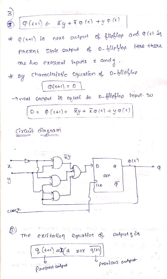
 PROBLEM 3 (16 PTS) ▪ With a D
flip flop and logic gates, sketch the circuit whose excitation
equation is given by:
PROBLEM 3 (16 PTS) ▪ With a D
flip flop and logic gates, sketch the circuit whose excitation
equation is given by:
Homework Answers

Add Answer to:
PROBLEM 3 (16 PTS) ▪ With a D
flip flop and logic gates, sketch the circuit...
Show how a D flip-flop can be constructed using a T flip-flop and other logic gates....
Show how a D flip-flop can be constructed using a T flip-flop and other logic gates. Provide the circuit, characteristic table and a timing diagram to demonstrate the operation (generate your own inputs).
Using all D flip-flops and combinational logic (AND/OR/NOT gates only) b) using all T flip-flop...
 using all D flip-flops and combinational logic (AND/OR/NOT gates
only)
b) using all T flip-flops and a multiplexer of size 8:1
Problem 3: (10 pts) Design a synchronous machine (Transition Table, K-maps, Final Equations, Circuit Diagram) that counts through the following sequence in the order shown below. Note, there are no inputs or output variables, so your Q values must reflect the Hex value listed B 74 2 D9 3 0 and repeat a) using all D flip-flops and combinational...
using all D flip-flops and combinational logic (AND/OR/NOT gates
only)
b) using all T flip-flops and a multiplexer of size 8:1
Problem 3: (10 pts) Design a synchronous machine (Transition Table, K-maps, Final Equations, Circuit Diagram) that counts through the following sequence in the order shown below. Note, there are no inputs or output variables, so your Q values must reflect the Hex value listed B 74 2 D9 3 0 and repeat a) using all D flip-flops and combinational...
(20 pts.) For the following circuit, the timing characteristics of the components are summarized below. .Flip-flop:...
 (20 pts.) For the following circuit, the timing characteristics of the components are summarized below. .Flip-flop: clock-to-Q maximum delay tpcq 40ps, clock-to-Q minimum delay tec 30ps, setup time tsetup 50ps, hold time thold 60ps Logic gate (each AND, OR, Inverter): propagation delay tpd 35ps, contamination delay ted25ps. FFl Fr3 CLK OUT FF2 CLK Suppose that there is no clock skew. What is the maximum clock frequency of this a. circuit? b. How much clock skew can the circuit tolerate before...
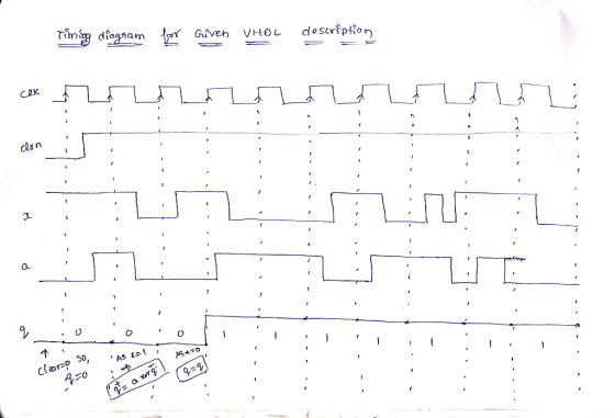
Use the Quartus Prime Text Editor to implement a behavioral model of the D flip-flop described ab...
 Use the Quartus Prime Text Editor to implement a behavioral
model of the D flip-flop described above in a file named
d_flops.sv. Specify the D flip-flop’s module according to the
interface specification given in the table below.
Port
Mode
Data Type
Size
Description
RST
in
logic
1-bit
Active high asynchronous reset
CLK
in
logic
1-bit
Synchronizing clock signal
EN
in
logic
1-bit
Synchronous clock enable
D
in
logic
1-bit
Synchronous data input
Q
out
logic
1-bit
Current/present state
Qbar
out...
Use the Quartus Prime Text Editor to implement a behavioral
model of the D flip-flop described above in a file named
d_flops.sv. Specify the D flip-flop’s module according to the
interface specification given in the table below.
Port
Mode
Data Type
Size
Description
RST
in
logic
1-bit
Active high asynchronous reset
CLK
in
logic
1-bit
Synchronizing clock signal
EN
in
logic
1-bit
Synchronous clock enable
D
in
logic
1-bit
Synchronous data input
Q
out
logic
1-bit
Current/present state
Qbar
out...
 using all D flip-flops and combinational logic (AND/OR/NOT gates
only)
b) using all T flip-flops and a multiplexer of size 8:1
Problem 3: (10 pts) Design a synchronous machine (Transition Table, K-maps, Final Equations, Circuit Diagram) that counts through the following sequence in the order shown below. Note, there are no inputs or output variables, so your Q values must reflect the Hex value listed B 74 2 D9 3 0 and repeat a) using all D flip-flops and combinational...
using all D flip-flops and combinational logic (AND/OR/NOT gates
only)
b) using all T flip-flops and a multiplexer of size 8:1
Problem 3: (10 pts) Design a synchronous machine (Transition Table, K-maps, Final Equations, Circuit Diagram) that counts through the following sequence in the order shown below. Note, there are no inputs or output variables, so your Q values must reflect the Hex value listed B 74 2 D9 3 0 and repeat a) using all D flip-flops and combinational...
 (20 pts.) For the following circuit, the timing characteristics of the components are summarized below. .Flip-flop: clock-to-Q maximum delay tpcq 40ps, clock-to-Q minimum delay tec 30ps, setup time tsetup 50ps, hold time thold 60ps Logic gate (each AND, OR, Inverter): propagation delay tpd 35ps, contamination delay ted25ps. FFl Fr3 CLK OUT FF2 CLK Suppose that there is no clock skew. What is the maximum clock frequency of this a. circuit? b. How much clock skew can the circuit tolerate before...
 Use the Quartus Prime Text Editor to implement a behavioral
model of the D flip-flop described above in a file named
d_flops.sv. Specify the D flip-flop’s module according to the
interface specification given in the table below.
Port
Mode
Data Type
Size
Description
RST
in
logic
1-bit
Active high asynchronous reset
CLK
in
logic
1-bit
Synchronizing clock signal
EN
in
logic
1-bit
Synchronous clock enable
D
in
logic
1-bit
Synchronous data input
Q
out
logic
1-bit
Current/present state
Qbar
out...
Use the Quartus Prime Text Editor to implement a behavioral
model of the D flip-flop described above in a file named
d_flops.sv. Specify the D flip-flop’s module according to the
interface specification given in the table below.
Port
Mode
Data Type
Size
Description
RST
in
logic
1-bit
Active high asynchronous reset
CLK
in
logic
1-bit
Synchronizing clock signal
EN
in
logic
1-bit
Synchronous clock enable
D
in
logic
1-bit
Synchronous data input
Q
out
logic
1-bit
Current/present state
Qbar
out...
Most questions answered within 3 hours.
-
Where is the error in this code sequence?
String s1 = "Hello";
String s2 = "ello";...
asked 10 months ago -
Financial data for Joel de Paris, Inc., for last year
follow:
Joel de Paris, Inc.
Balance...
asked 10 months ago -
Consider this reaction:
Al2(SO4)3 (aq)+ BaCl3
(aq) Al2Cl6 (aq)- +
3BaSO4(s) . What is the...
asked 10 months ago -
Suppose that Savneet is considering increasing her
recent random sample from 20 car rentals to 40...
asked 10 months ago -
Trucks arrive at an unloading terminal at an average rate of 120
per hour.
Trucks arrive...
asked 10 months ago -
Why are methanol and ethanol completely soluble in water while
octanol is not very little soluble....
asked 10 months ago -
A facilities manager at a university reads in a research report
that the mean amount of...
asked 10 months ago -
When the CuSO4 is rehydrated by adding water to the anhydrous
compound, is this an endothermic...
asked 10 months ago -
A ray of sunlight is passing from diamond into crown glass; the
angle of incidence is...
asked 10 months ago -
A block of mass 0.249 kg is placed on top of a light, vertical
spring of...
asked 10 months ago -
how do the kidneys compensate in the presences of acidosis
a) trigger hyperventilate
b) reserve acid...
asked 10 months ago -
Question 501 pts
The rental rate of capital to the firm increases. Which of the
following...
asked 10 months ago