Let f(w, x, y, z) = Q M(4, 9, 12, 13, 14) and d(w, x, y,...
Let f(w, x, y, z) = Q M(4, 9, 12, 13, 14) and d(w, x, y, z) = P m(5, 6, 11, 15). {[d(w, x, y, z) defines the don’t care conditions of f}.
(a) (10pts) Find the minimal SOP of f.
(b) (10pts) Find the minimal POS of f.
(c) (20pts) Design a circuit from the minimal SOP of f. The circuit should contain only NAND gates
Homework Answers
a)
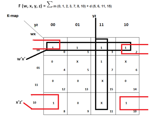
The minimal SOP of f = w’x’+x’z’+yz
b)
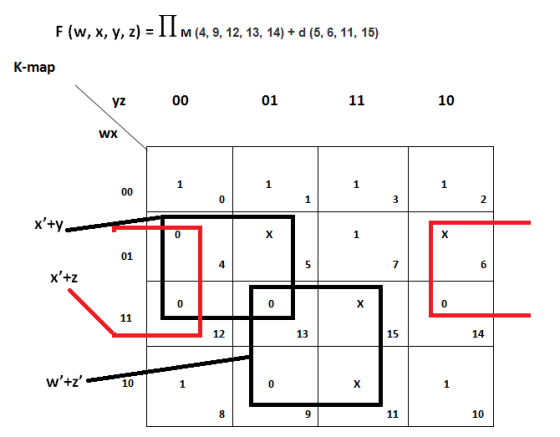
The minimal POS of f = (x’+y)(w’+z’)(x'+z)
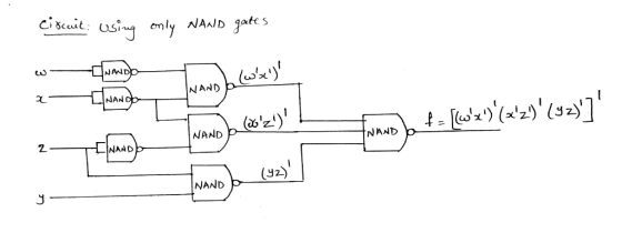
c) Given f = w’x’+x’z’+yz
(f')' = [( w’x’+x’z’+yz)']'
f = [( w’x’)' (x’z’)' (yz)']'
Q2: 1. Proof this Boolean expression. Use Boolean Algebra (X+Y). (Z+W).(X'+Y+W) = Y.Z+X.W+Y.W 2. For this...
 Q2: 1. Proof this Boolean expression. Use Boolean Algebra (X+Y). (Z+W).(X'+Y+W) = Y.Z+X.W+Y.W 2. For this BF F(X,,Z)=((XYZ)(X +Z))(X+Y) • Design the digital circuit Derive the Boolean Function of X, Y, Z. Simplify the Function Derive the truth table before and after simplification. Derive the BF F(X,Y,Z) as Maxterms (POS) and miterms (SOP). Implement the F(X,Y,Z) after simplification using NAND gates only. Implement the F(X,Y,Z) after simplification using OR NOR gates only.
Implement the Boolean function F(w,x,y,z) = Σm(3, 4, 5, 1 1, 12, 13, 14, 15) using a minimum number of NAND gates only.
Implement the Boolean function F(w,x,y,z) = Σm(3, 4, 5, 1 1, 12, 13, 14, 15) using a minimum number of NAND gates only. Write the minimal logic expression (no need to draw the circuit).
Q3: 1. For the Boolean function shown below, answer the questions F(W,X,Y,Z) = 11 (6,8,9,10,11,12,13) use...
 Q3: 1. For the Boolean function shown below, answer the questions F(W,X,Y,Z) = 11 (6,8,9,10,11,12,13) use K-MAP to: • Derive the BF as SOP. • Derive the BF as POS. • Find All prime implicants of the BF. • Determine the Essential prime implicant(s). 2. Let the BF change to have don't care condition as: F(W,X,Y,Z) = 1,3,7,11,15 + de E(0.2,5) Derive the BF as SOP and POS.
Consider the following logic: F = ΣW,X,Y,Z (0x1, 0x5, 0x8, 0xA, 0xB, 0xC, 0xE, 0xF). And...
Consider the following logic: F = ΣW,X,Y,Z (0x1, 0x5, 0x8, 0xA, 0xB, 0xC, 0xE, 0xF). And 0x2, 0x4 and 0x6 are “don't care” cases. a) Draw a K-map and write a minimized SOP expression for this circuit. Include grouping circles for a minimized SOP expression. b) Draw the minimized SOP circuit using only NAND gates. c) Are there any static hazards? If so, write the Boolean expression to resolve any static hazards?
QUESTION 1 [TOTAL MARKS:25] A manufacturing process has four sensors labelled W.X, Y. and Z. The...
 QUESTION 1 [TOTAL MARKS:25] A manufacturing process has four sensors labelled W.X, Y. and Z. The system should sound an alarm if any of the following conditions arise: • W, X, Y, Z are not activated at the same time. • X, Y, and Z are not activated and W is activated at the same time. • Wand Y are not activated, and X and Z are activated at the same time. • W, X, and Z are not activated,...
Q31 For the figure shown below W is an input, (X, Y and Z) are connected...
 Q31 For the figure shown below W is an input, (X, Y and Z) are connected to (S2, S and So), find the Boolean function F (W, X, Y, Z) in SOP and implement it use: 1. Multiplexer: One-piece (4 to 1) and external gates (W, X are selectors). 2. Decoder: Five (2 to 4) with AND gate. 0 1 8 to 1 MUX Do D, F OP D, S S S 35 Marks] X Y Z
Q31 For the...
Q31 For the figure shown below W is an input, (X, Y and Z) are connected to (S2, S and So), find the Boolean function F (W, X, Y, Z) in SOP and implement it use: 1. Multiplexer: One-piece (4 to 1) and external gates (W, X are selectors). 2. Decoder: Five (2 to 4) with AND gate. 0 1 8 to 1 MUX Do D, F OP D, S S S 35 Marks] X Y Z
Q31 For the...
1. (8 points) Obtain a minimal SOP form for the boolean function f(x,y,z,w) implemented by logic...
 1. (8 points) Obtain a minimal SOP form for the boolean function f(x,y,z,w) implemented by logic network below. Compare the gate count and number of gate inputs in your minimal SOP expression with those for the network below. f(x,y,z,w)
Write the Boolean expression that implements the function, F(W,X,Y,Z) = ∑m(1,7,8,10,13) as a 4. NAND-NAND circuit...
Write the Boolean expression that implements the function, F(W,X,Y,Z) = ∑m(1,7,8,10,13) as a 4. NAND-NAND circuit 5. OR-NAND circuit 6. NOR-OR 7. Construct the truth table, K-map minimization, boolean expressions and circuit diagrams for all output bits of a circuit that performs 1’s complement of a 4-bit binary number. Assume overflow bits are lost:
We are interested in designing a circuit that implements the following three Boolean functions: 3. h(x,y,z)=Σm(1,4,6)...
 We are interested in designing a circuit that implements the following three Boolean functions: 3. h(x,y,z)=Σm(1,4,6) f1x,y,z)- > m(1,4,6) y-m35) (x,y, z) Σ m (2,4,6,7) 左 You are supposed to implement the circuit with a decoder constructed with NAND gates (a) [12pt] Start by drawing the block diagram of a NAND-based decoder with three inputs (x,y,z), labelling all the outputs with their corresponding Boolean functions (b) [8pt) Using a new block diagram of the NAND-based decoder, implement the circuit using...
I would like to know if the SOP function f(v,w,x,y,z)=(x+z)(w+y)(!w+x+!y)(!y+z+!v) and The Quartus II obtained function...
I would like to know if the SOP function f(v,w,x,y,z)=(x+z)(w+y)(!w+x+!y)(!y+z+!v) and The Quartus II obtained function F(v,w,x,y,z)=(v((!x(z(!w xor (!y))))+(x((!y(w))+(y((z)))))))+(!v((!x(z(!w xor (!y))))+(x(((y))+(w))))) for the above SOP are equivalent?
 Q2: 1. Proof this Boolean expression. Use Boolean Algebra (X+Y). (Z+W).(X'+Y+W) = Y.Z+X.W+Y.W 2. For this BF F(X,,Z)=((XYZ)(X +Z))(X+Y) • Design the digital circuit Derive the Boolean Function of X, Y, Z. Simplify the Function Derive the truth table before and after simplification. Derive the BF F(X,Y,Z) as Maxterms (POS) and miterms (SOP). Implement the F(X,Y,Z) after simplification using NAND gates only. Implement the F(X,Y,Z) after simplification using OR NOR gates only.
 Q3: 1. For the Boolean function shown below, answer the questions F(W,X,Y,Z) = 11 (6,8,9,10,11,12,13) use K-MAP to: • Derive the BF as SOP. • Derive the BF as POS. • Find All prime implicants of the BF. • Determine the Essential prime implicant(s). 2. Let the BF change to have don't care condition as: F(W,X,Y,Z) = 1,3,7,11,15 + de E(0.2,5) Derive the BF as SOP and POS.
 QUESTION 1 [TOTAL MARKS:25] A manufacturing process has four sensors labelled W.X, Y. and Z. The system should sound an alarm if any of the following conditions arise: • W, X, Y, Z are not activated at the same time. • X, Y, and Z are not activated and W is activated at the same time. • Wand Y are not activated, and X and Z are activated at the same time. • W, X, and Z are not activated,...
 Q31 For the figure shown below W is an input, (X, Y and Z) are connected to (S2, S and So), find the Boolean function F (W, X, Y, Z) in SOP and implement it use: 1. Multiplexer: One-piece (4 to 1) and external gates (W, X are selectors). 2. Decoder: Five (2 to 4) with AND gate. 0 1 8 to 1 MUX Do D, F OP D, S S S 35 Marks] X Y Z
Q31 For the...
Q31 For the figure shown below W is an input, (X, Y and Z) are connected to (S2, S and So), find the Boolean function F (W, X, Y, Z) in SOP and implement it use: 1. Multiplexer: One-piece (4 to 1) and external gates (W, X are selectors). 2. Decoder: Five (2 to 4) with AND gate. 0 1 8 to 1 MUX Do D, F OP D, S S S 35 Marks] X Y Z
Q31 For the...
 1. (8 points) Obtain a minimal SOP form for the boolean function f(x,y,z,w) implemented by logic network below. Compare the gate count and number of gate inputs in your minimal SOP expression with those for the network below. f(x,y,z,w)
 We are interested in designing a circuit that implements the following three Boolean functions: 3. h(x,y,z)=Σm(1,4,6) f1x,y,z)- > m(1,4,6) y-m35) (x,y, z) Σ m (2,4,6,7) 左 You are supposed to implement the circuit with a decoder constructed with NAND gates (a) [12pt] Start by drawing the block diagram of a NAND-based decoder with three inputs (x,y,z), labelling all the outputs with their corresponding Boolean functions (b) [8pt) Using a new block diagram of the NAND-based decoder, implement the circuit using...
Most questions answered within 3 hours.
-
Where is the error in this code sequence?
String s1 = "Hello";
String s2 = "ello";...
asked 11 months ago -
Financial data for Joel de Paris, Inc., for last year
follow:
Joel de Paris, Inc.
Balance...
asked 11 months ago -
Consider this reaction:
Al2(SO4)3 (aq)+ BaCl3
(aq) Al2Cl6 (aq)- +
3BaSO4(s) . What is the...
asked 11 months ago -
Suppose that Savneet is considering increasing her
recent random sample from 20 car rentals to 40...
asked 11 months ago -
Trucks arrive at an unloading terminal at an average rate of 120
per hour.
Trucks arrive...
asked 11 months ago -
Why are methanol and ethanol completely soluble in water while
octanol is not very little soluble....
asked 11 months ago -
A facilities manager at a university reads in a research report
that the mean amount of...
asked 11 months ago -
When the CuSO4 is rehydrated by adding water to the anhydrous
compound, is this an endothermic...
asked 11 months ago -
A ray of sunlight is passing from diamond into crown glass; the
angle of incidence is...
asked 11 months ago -
A block of mass 0.249 kg is placed on top of a light, vertical
spring of...
asked 11 months ago -
how do the kidneys compensate in the presences of acidosis
a) trigger hyperventilate
b) reserve acid...
asked 11 months ago -
Question 501 pts
The rental rate of capital to the firm increases. Which of the
following...
asked 11 months ago