Create the following circuits in Logisim as you have seen the instructor do on the lectures....
- Create the following circuits in
Logisim as you have seen the instructor
do on the lectures. DO NOT use built-in MUX, ADDER or D-Latch for
this.
- A 6-to-1 mux using basic gates (AND, OR)
- A four-bit full adder. Create a 1-bit adder first and then use it as a block to create a four-bit adder.
- A 1 bit gated D-Latch and then reuse it to as a block create a two-bit D-Latch.
Homework Answers
Following circuits are designed using Logisim, Here we have not used the built-in MUX, ADDER or D-Latch
a) A 6-to-1 MUX using basic gates:
A 6-to-1 MUX will have six inputs and one output. This circuit will require 3 select inputs. Here S2 S1 S0 are the three select inputs, and I0 I1, I2, I3, I4, and I5 are the six inputs of a 6-to-1 multiplexer. Depending on the value in the select input, one input will be selected and passed to the output.
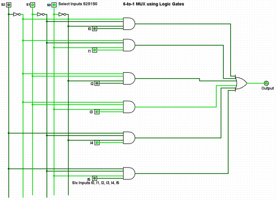
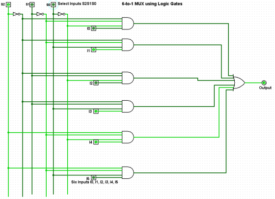
The following logisim diagram shows a 6-to-1 MUX designed using basic logic gates.
The truth table of a 6:1 MUX that used for the deisgn is given below:

The output is the OR of multiple AND terms. Here the first AND term from the truth table is S2'S1'S0'I0
Similarly, we can find the other AND terms to obtain the circuit of 6:1 MUX.
Here, the select inputs are shown as 000 and the output is I0 or the value of the I0 input which is 0 here

When select input S2S1S0=001 then the output is I1 or the value of the I1 input which is 1 here
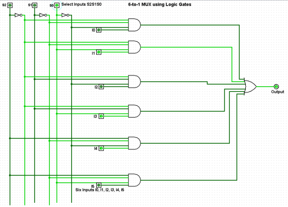
When select input S2S1S0=010 then the output is I2 or the value of the I2 input which is 0 here

When select input S2S1S0=011 then the output is I3 or the value of the I3 input which is 1 here
When select input S2S1S0=100 then the output is I4 or the value of the I4 input which is 1 here
When select input S2S1S0=101 then the output is I5 or the value of the I5 input which is 0 here

Here care must be taken not to give 110 and 111 as the select inputs, as these are invalid select inputs for a 6-to-1 MUX.
b) A four-bit full adder using four 1-bit adders
We will design a one-bit adder circuit that will add two one-bit numbers A and B and will output the sum and carry.
The truth table of a one-bit full adder is shown below:

This circuit designed using logisim using logic gates is shown below:

This 1-bit full adder will add two 1-bit numbers (A and B) and product the sum output bit and a carry output bit. Provision is made to add the input carry C also if any. If there is no input carry this C input bit will always be 0.
Now we can use the above one-bit adder as a block to create a four-bit adder. We have used the four blocks of one-bit full adder designed earlier to design this four-fit full adder in logisim as shown below:

Here two four-bit numbers A3A2A1A0 is added with B3B2B1B0 to obtain the output S3S2S1S0 along with a carry output Cout
Also, the addition of two four-bit numbers 1001 + 1101 is shown below in the logisim circuit, the input and output can be observed. The output is 0110 with an output carry of 1. This is illustrated in the following diagram:

c) A 1 bit gated D-Latch and then reuse it to as a block create a two-bit D-Latch
The 1-bit gated D-latch is shown below designed using logisim:

Here, the circuit is enabled or made active when we give logic 1 to the Enable input.
When D=0, Q=0 and
when D=1, Q=1
Now, we can reuse this to design a 2-bit gated D-latch in logisim as shown below:

Here, in the 2-bit gated latch, two input bits are D0 D1 and the outputs are Q0 Q1
Add Answer to:
Create the following circuits in
Logisim as you have seen the instructor
do on the lectures....
Using logisim to create a 4bit controlled comparator ECFICATIONS NPUTS Create a cireuit in Logisi...
 Using logisim to create a 4bit controlled comparator ECFICATIONS NPUTS Create a cireuit in Logisim thait will take the following inputs 4 bit binary number :4 bit binary number Control where C-O, A and B will be treated as unsigned binary C-1,A and B will be treated as 2's complement signed binary (for example, the number 301 represents the value 5' it is treated as unsigned binary but it represents the value - if it is treated as 2's complemene...
Building and testing basic combinational circuits using Verilog HDL Description: Build and test the following circuits using gate-level modeling in Verilog HDL 1.3-input majority function 2.Condition...
 Building and testing basic combinational circuits using Verilog HDL Description: Build and test the following circuits using gate-level modeling in Verilog HDL 1.3-input majority function 2.Conditional inverter (see the table below: x - control input, y -data input). Do NOT use XOR gates for the implementation. Output 3. Two-input multiplexer (see the table below: x.y -data inputs, z- control input) Output 4. 1-bit half adder. 5. 1-bit full adder by cascading two half adders 6.1-bit full adder directly (as in...
Building and testing basic combinational circuits using Verilog HDL Description: Build and test t...
Building and testing basic combinational circuits using Verilog HDL Description: Build and test the following circuits using gate-level modeling in Verilog HDL. 1. 3-input majority function. 2. Conditional inverter (see the table below: x - control input, y - data input). Do NOT use XOR gates for the implementation. x y Output 0 y 1 y' 3. Two-input multiplexer (see the table below: x,y - data inputs, z - control input). z Output 0 x 1 y 4. 1-bit half...
First you must create a logic circuit using only basic gates such as AND, OR, NOR,...
First you must create a logic circuit using only basic gates such as AND, OR, NOR, NAND, NOT, etc. to implement an ADDER capable of adding two 4 bit binary numbers. Second you must create a logic circuit using only basic gates such as AND, OR, NOR, NAND, NOT, etc. to implement a Subtractor that is capable of subtracting the second number from the first, by converting the second number into its 2's complement form and then adding the resulting...
1. Use both circuits and incorporate a carry in using basic gates to get a 1...
 1. Use both circuits and incorporate a carry in using
basic gates to get a 1 bit full adder.
2. Using the prior circuit, modify it to make a 3 bit
adder that can add the two’s complement of the 2nd input (i.e. be
able to subtract).
I have drawn two gates, one is used to (i)"calculate the sum of
two bits using basic gates." while the other is used to (ii)"carry
out for the sum of two bits using...
1. Use both circuits and incorporate a carry in using
basic gates to get a 1 bit full adder.
2. Using the prior circuit, modify it to make a 3 bit
adder that can add the two’s complement of the 2nd input (i.e. be
able to subtract).
I have drawn two gates, one is used to (i)"calculate the sum of
two bits using basic gates." while the other is used to (ii)"carry
out for the sum of two bits using...
3. Digital circuits question. The figure below shows a 16-b carry-skip adder. It is composed of...
 3. Digital circuits question.
The figure below shows a 16-b carry-skip adder. It is composed of 4 4-bit ripple carry adders and some extra logic to route the carry. Each 4bit ripple carry adder generates a group propagate signal. This is used to determine when the carry-in is going to be propagated all the way to the carry-out. When this is the case, addition is sped up by allowing the carry-in to skip the block and become the carry-in of...
3. Digital circuits question.
The figure below shows a 16-b carry-skip adder. It is composed of 4 4-bit ripple carry adders and some extra logic to route the carry. Each 4bit ripple carry adder generates a group propagate signal. This is used to determine when the carry-in is going to be propagated all the way to the carry-out. When this is the case, addition is sped up by allowing the carry-in to skip the block and become the carry-in of...
FPGA (Interconnected Adder Modules) In this lab you will implement adder circuits using data flow modelling....
FPGA (Interconnected Adder Modules) In this lab you will implement adder circuits using data flow modelling. You will also create 3-bit adder by employing interconnected 1-bit full adders. Data flow modelling of a 1-bit full adder circuit. Data flow modelling of a 3-bit adder circuit. There will be 7 inputs (X2, X1, X0, Y2, Y1, YO, Cin) - please put them in that order - Switch 6 will represent X2 and Switch 0 will be the Cin. There should be...
(Don't do the simulation If you don't have LigoSim to simulate) I appreciate your efforts and...
(Don't do the simulation If you don't have LigoSim to simulate) I appreciate your efforts and time in advance! a)Simulate and test a 1-bit full adder. Use 2-input exclusive OR gates to realize Sum. Use an SOP form to realize Cout b) Simulate and test a 4-bit adder circuit using serially interconnected 1-bit full adder sub-circuits. The adder will be able to add 4 bit positive numbers and should be able to add 15 and 15 to get 30. c)...
8/8pts Question 1 Using block diagram of 1-bit full adders create a 3-bit parallel adder (show...
 8/8pts Question 1 Using block diagram of 1-bit full adders create a 3-bit parallel adder (show all the connections between the adders and proper outputs Logic Q1jpg 4/9 pts Question 2 Consider your design, if the inputs to be added were 100, and 111, what will be the resulting sum output (Express the resulting sum in binary and base 8 using the least number of bits)? What will be the carry output (Express it only in binary using the least...
4 BIT ALU due 4/24 Midnight Implement a 4 bit ALU as covered in class. INPUTS:...
4 BIT ALU due 4/24 Midnight Implement a 4 bit ALU as covered in class. INPUTS: A – 4 bit 2’s complement number B – 4 bit 2’s complement number Control – determines ALU functionality OUTPUT: If control = 00, then output = A AND B If control = 01, then output = A OR B If control = 10, then output = A ADD B If control = 11, then output = A SUBTRACT B REQUIREMENTS: 1) You are...
 Using logisim to create a 4bit controlled comparator ECFICATIONS NPUTS Create a cireuit in Logisim thait will take the following inputs 4 bit binary number :4 bit binary number Control where C-O, A and B will be treated as unsigned binary C-1,A and B will be treated as 2's complement signed binary (for example, the number 301 represents the value 5' it is treated as unsigned binary but it represents the value - if it is treated as 2's complemene...
 Building and testing basic combinational circuits using Verilog HDL Description: Build and test the following circuits using gate-level modeling in Verilog HDL 1.3-input majority function 2.Conditional inverter (see the table below: x - control input, y -data input). Do NOT use XOR gates for the implementation. Output 3. Two-input multiplexer (see the table below: x.y -data inputs, z- control input) Output 4. 1-bit half adder. 5. 1-bit full adder by cascading two half adders 6.1-bit full adder directly (as in...
 1. Use both circuits and incorporate a carry in using
basic gates to get a 1 bit full adder.
2. Using the prior circuit, modify it to make a 3 bit
adder that can add the two’s complement of the 2nd input (i.e. be
able to subtract).
I have drawn two gates, one is used to (i)"calculate the sum of
two bits using basic gates." while the other is used to (ii)"carry
out for the sum of two bits using...
1. Use both circuits and incorporate a carry in using
basic gates to get a 1 bit full adder.
2. Using the prior circuit, modify it to make a 3 bit
adder that can add the two’s complement of the 2nd input (i.e. be
able to subtract).
I have drawn two gates, one is used to (i)"calculate the sum of
two bits using basic gates." while the other is used to (ii)"carry
out for the sum of two bits using...
 3. Digital circuits question.
The figure below shows a 16-b carry-skip adder. It is composed of 4 4-bit ripple carry adders and some extra logic to route the carry. Each 4bit ripple carry adder generates a group propagate signal. This is used to determine when the carry-in is going to be propagated all the way to the carry-out. When this is the case, addition is sped up by allowing the carry-in to skip the block and become the carry-in of...
3. Digital circuits question.
The figure below shows a 16-b carry-skip adder. It is composed of 4 4-bit ripple carry adders and some extra logic to route the carry. Each 4bit ripple carry adder generates a group propagate signal. This is used to determine when the carry-in is going to be propagated all the way to the carry-out. When this is the case, addition is sped up by allowing the carry-in to skip the block and become the carry-in of...
 8/8pts Question 1 Using block diagram of 1-bit full adders create a 3-bit parallel adder (show all the connections between the adders and proper outputs Logic Q1jpg 4/9 pts Question 2 Consider your design, if the inputs to be added were 100, and 111, what will be the resulting sum output (Express the resulting sum in binary and base 8 using the least number of bits)? What will be the carry output (Express it only in binary using the least...
Most questions answered within 3 hours.
-
Where is the error in this code sequence?
String s1 = "Hello";
String s2 = "ello";...
asked 11 months ago -
Financial data for Joel de Paris, Inc., for last year
follow:
Joel de Paris, Inc.
Balance...
asked 11 months ago -
Consider this reaction:
Al2(SO4)3 (aq)+ BaCl3
(aq) Al2Cl6 (aq)- +
3BaSO4(s) . What is the...
asked 11 months ago -
Suppose that Savneet is considering increasing her
recent random sample from 20 car rentals to 40...
asked 11 months ago -
Trucks arrive at an unloading terminal at an average rate of 120
per hour.
Trucks arrive...
asked 11 months ago -
Why are methanol and ethanol completely soluble in water while
octanol is not very little soluble....
asked 11 months ago -
A facilities manager at a university reads in a research report
that the mean amount of...
asked 11 months ago -
When the CuSO4 is rehydrated by adding water to the anhydrous
compound, is this an endothermic...
asked 11 months ago -
A ray of sunlight is passing from diamond into crown glass; the
angle of incidence is...
asked 11 months ago -
A block of mass 0.249 kg is placed on top of a light, vertical
spring of...
asked 11 months ago -
how do the kidneys compensate in the presences of acidosis
a) trigger hyperventilate
b) reserve acid...
asked 11 months ago -
Question 501 pts
The rental rate of capital to the firm increases. Which of the
following...
asked 11 months ago