
Homework Answers

Add Answer to:
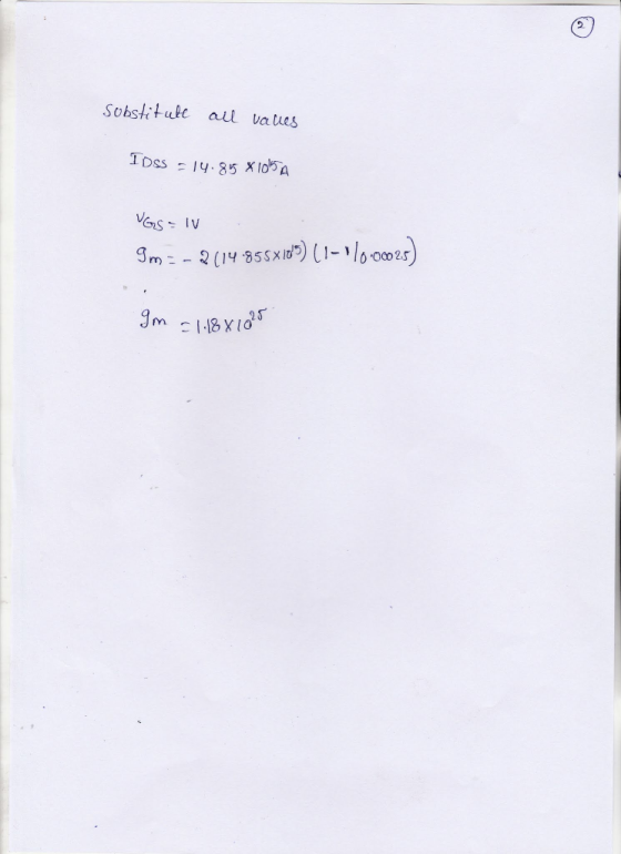
Special Problem (20 pts) Design a one-sided GaAs n-channel MESFET with a barrier height of φΒη-0....
Problem 3 An n-channel MOSFET with L=1 um, W=3 um, tox=20 nm, V=0.7 V, and an...
 Problem 3 An n-channel MOSFET with L=1 um, W=3 um, tox=20 nm, V=0.7 V, and an effective electron mobility in the channel of 650 cm/V-s. a) If the MOSFET is biased with VG-V=3V, and Vp=2V, what is the drain current and transconductance of this MOSFET? b) Assume long channel theory is valid, what are (i) the velocities of channel carriers at the source and drain? (ii) the output resistance of the MOSFET? c) Plot channel conductance (ga) versus VG for...
Special Problem (20 pts) Consider an undoped AljGa7As/GaAs/ Al3Ga7As quantum well (QW) of width W...
 Special Problem (20 pts) Consider an undoped AljGa7As/GaAs/ Al3Ga7As quantum well (QW) of width W-15 nm. (a) Due the quantum mechanical confinement in the quantum well, the lowest energy states of in the conduction band is no longer the conduction band edge, but the CB edge plus the confined state energy (particle in the box problem), where the confinement energy relative to the CB edge is given by the solutions for infinite barriers where n-1,2,.is the quantum number, n-1 is...
Problem 3: Design Problem On Figure P3a, you have a Common Source (CS) n-channel MOSFET amplifier....
 Problem 3: Design Problem On Figure P3a, you have a Common Source (CS) n-channel MOSFET amplifier. Notice the absence of a source resistor Rsig and load resistor R. If we know how the present amplifier (the one on Figure P3a) behaves without Rsig and RL, we can infer its behaviors if Rsig and R were to be added. design the amplifier circuit on Figure P3a, i.e., you have to find appropriate values for RGj You are to RG,, RD, and...
 Problem 3 An n-channel MOSFET with L=1 um, W=3 um, tox=20 nm, V=0.7 V, and an effective electron mobility in the channel of 650 cm/V-s. a) If the MOSFET is biased with VG-V=3V, and Vp=2V, what is the drain current and transconductance of this MOSFET? b) Assume long channel theory is valid, what are (i) the velocities of channel carriers at the source and drain? (ii) the output resistance of the MOSFET? c) Plot channel conductance (ga) versus VG for...
 Special Problem (20 pts) Consider an undoped AljGa7As/GaAs/ Al3Ga7As quantum well (QW) of width W-15 nm. (a) Due the quantum mechanical confinement in the quantum well, the lowest energy states of in the conduction band is no longer the conduction band edge, but the CB edge plus the confined state energy (particle in the box problem), where the confinement energy relative to the CB edge is given by the solutions for infinite barriers where n-1,2,.is the quantum number, n-1 is...
 Problem 3: Design Problem On Figure P3a, you have a Common Source (CS) n-channel MOSFET amplifier. Notice the absence of a source resistor Rsig and load resistor R. If we know how the present amplifier (the one on Figure P3a) behaves without Rsig and RL, we can infer its behaviors if Rsig and R were to be added. design the amplifier circuit on Figure P3a, i.e., you have to find appropriate values for RGj You are to RG,, RD, and...
Most questions answered within 3 hours.
-
Where is the error in this code sequence?
String s1 = "Hello";
String s2 = "ello";...
asked 10 months ago -
Financial data for Joel de Paris, Inc., for last year
follow:
Joel de Paris, Inc.
Balance...
asked 10 months ago -
Consider this reaction:
Al2(SO4)3 (aq)+ BaCl3
(aq) Al2Cl6 (aq)- +
3BaSO4(s) . What is the...
asked 10 months ago -
Suppose that Savneet is considering increasing her
recent random sample from 20 car rentals to 40...
asked 10 months ago -
Trucks arrive at an unloading terminal at an average rate of 120
per hour.
Trucks arrive...
asked 10 months ago -
Why are methanol and ethanol completely soluble in water while
octanol is not very little soluble....
asked 10 months ago -
A facilities manager at a university reads in a research report
that the mean amount of...
asked 10 months ago -
When the CuSO4 is rehydrated by adding water to the anhydrous
compound, is this an endothermic...
asked 10 months ago -
A ray of sunlight is passing from diamond into crown glass; the
angle of incidence is...
asked 10 months ago -
A block of mass 0.249 kg is placed on top of a light, vertical
spring of...
asked 10 months ago -
how do the kidneys compensate in the presences of acidosis
a) trigger hyperventilate
b) reserve acid...
asked 10 months ago -
Question 501 pts
The rental rate of capital to the firm increases. Which of the
following...
asked 10 months ago