
Homework Answers
Add Answer to:
(Optional, 12 bonus points) Consider a imensional semiconductor with a band structure as shown in...
Band structure Consider a one-dimensional semiconductor crystal consisting of 11 atoms with nearest- neighbor atoms separated...
 Band structure Consider a one-dimensional semiconductor crystal consisting of 11 atoms with nearest- neighbor atoms separated by a 5 . The band structure for electrons in the conduction band is given by Ec(k) = 101(k-0.2n)2-A(k-02n)"] + 2.25 [eV] and the band structure for holes in the valence band is given by where the wavevector k s in units ofA-1. The allowed wavevectors are--< k 즈 al (a) Is this a direct or indirect gap semiconductor? What is the energy gap...
A) Show that the chemical potential in an intrinsic semiconductor lies in the middle of the gap a...
a) Show that the chemical potential in an intrinsic semiconductor lies in the middle of the gap at low temperature. (b) Explain how the chemical potential varies with temperature if the semiconductor is doped with (i) donors (ii) acceptors. (c) A direct-gap semiconductor is doped to produce a density of 1023electrons/m3. Calculate the hole density at room temperature given that the gap is 1.0 eV, and the effective mass of carriers in the conduction and valence band are 0.25 and...
Consider a GaAs semiconductor at room temperature (T = 300 K). The bandgap energy is Eg...
Consider a GaAs semiconductor at room temperature (T = 300 K). The bandgap energy is Eg = 1.42 eV. The electron-to-hole effective mass ratio is me*/mh*=0.134. It is given that the separation between the Fermi level (located in the bandgap) and the top of the valence band is 4 times the separation between the bottom of the conduction band and the Fermi level. Find the ratio of the electron concentration in the conduction band to the hole concentration in the...
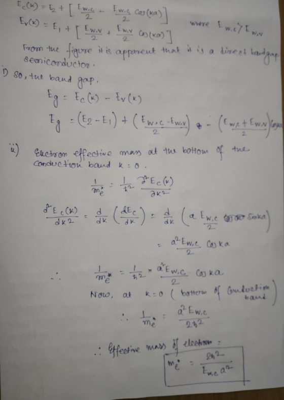
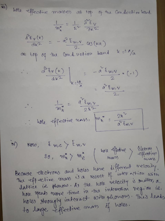
The band structure of an unknown semiconductor is given by Ec (k) = 20k2 - 20k...
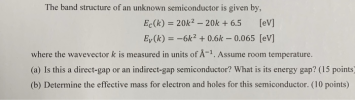 The band structure of an unknown semiconductor is given by Ec (k) = 20k2 - 20k +6.5 [eV] Ey (k) = 6k2 + 0.6k - 0.065 [eV] where the wavevector k is measured in units of A-1. Assume room temperature. (a) Is this a direct-gap or an indirect-gap semiconductor? What is its energy gap? (15 points) (b) Determine the effective mass for electron and holes for this semiconductor. (10 points)
The band structure of an unknown semiconductor is given by...
The band structure of an unknown semiconductor is given by Ec (k) = 20k2 - 20k +6.5 [eV] Ey (k) = 6k2 + 0.6k - 0.065 [eV] where the wavevector k is measured in units of A-1. Assume room temperature. (a) Is this a direct-gap or an indirect-gap semiconductor? What is its energy gap? (15 points) (b) Determine the effective mass for electron and holes for this semiconductor. (10 points)
The band structure of an unknown semiconductor is given by...
The band structure of an unknown semiconductor is given by Ec (k) = 20k2 20k +6.5...
 The band structure of an unknown semiconductor is given by Ec (k) = 20k2 20k +6.5 [eV] Ey (k) = -6k2 +0.6k - 0.065 [eV] where the wavevector k is measured in units of A-1. Assume room temperature. (a) Is this a direct-gap or an indirect-gap semiconductor? What is its energy gap? (15 points) (b) Determine the effective mass for electron and holes for this semiconductor. (10 points)
The band structure of an unknown semiconductor is given by Ec (k)...
The band structure of an unknown semiconductor is given by Ec (k) = 20k2 20k +6.5 [eV] Ey (k) = -6k2 +0.6k - 0.065 [eV] where the wavevector k is measured in units of A-1. Assume room temperature. (a) Is this a direct-gap or an indirect-gap semiconductor? What is its energy gap? (15 points) (b) Determine the effective mass for electron and holes for this semiconductor. (10 points)
The band structure of an unknown semiconductor is given by Ec (k)...
A wire is made of an intrinsic semiconductor whose bandgap is 1.0eV. The wire is 0.05microns...
 A wire is made of an intrinsic semiconductor whose bandgap is 1.0eV. The wire is 0.05microns in diameter and 1 micron long. Electrons have a mobility of 1000/cm V-sec and holes have a mobility of 200/cm V-sec. The effective mass of an electron in the conduction band is 1.2 and that of a hole in the valence band is 0.6. The semiconductor operates at room temperature. a. What is the probability of finding an electron at an energy 0.5eV above...
semiconductor devices . Electron-hole recombination in direct band-gap semiconductors is known to yield photons. (0) For...
 semiconductor devices
. Electron-hole recombination in direct band-gap semiconductors is known to yield photons. (0) For which application this property is used? Explain briefly (ii) Calculate the primary wavelength of photons emitted from InP as a result of such recombination. (ii) Is it possible to see the emitted photons? Explain briefly (iv) Suppose you desire to detect the radiation from a GaP laser, can you use a Ge photodetector for that purpose? Explain briefly
semiconductor devices
. Electron-hole recombination in direct band-gap semiconductors is known to yield photons. (0) For which application this property is used? Explain briefly (ii) Calculate the primary wavelength of photons emitted from InP as a result of such recombination. (ii) Is it possible to see the emitted photons? Explain briefly (iv) Suppose you desire to detect the radiation from a GaP laser, can you use a Ge photodetector for that purpose? Explain briefly
Please explain part b in details thx! Question 2 At 300 K, the bandgap of GaP is 2.26 eV and the effective density of states at the conduction and valence band edge are 1.8 x 1019 cm23 and 1.9 x 10¹⁹...
 Please explain part b in details thx!
Question 2 At 300 K, the bandgap of GaP is 2.26 eV and the effective density of states at the conduction and valence band edge are 1.8 x 1019 cm23 and 1.9 x 1019 cm3, respectively. (a) Calculate the intrinsic concentration of GaP at 300K (7 marks) Calculate the GaP effective mass of holes at 300K. (b) (8 marks) (c The GaP sample is now doped with donor concentration of 1021 cm3 with...
Please explain part b in details thx!
Question 2 At 300 K, the bandgap of GaP is 2.26 eV and the effective density of states at the conduction and valence band edge are 1.8 x 1019 cm23 and 1.9 x 1019 cm3, respectively. (a) Calculate the intrinsic concentration of GaP at 300K (7 marks) Calculate the GaP effective mass of holes at 300K. (b) (8 marks) (c The GaP sample is now doped with donor concentration of 1021 cm3 with...
2. (a) Assuming Anderson's rule and Vegard's law calculate the depth of the confining potential in meV, for holes in the valence band of a InAs/InxGa1-xAs multi QW structure where x-0.5. [5]...
 2. (a) Assuming Anderson's rule and Vegard's law calculate the depth of the confining potential in meV, for holes in the valence band of a InAs/InxGa1-xAs multi QW structure where x-0.5. [5] State whether electron and hole confinement is within the InAs or InGaAs layers, and hence deduce what type of structure/band alignment this is. Suggest why this structure might be difficult to grow experimentally. (b) A Gao.47lno.53As quantum well laser is designed to emit at 1.55um at room temperature...
E(k)t Er K. 4. (Advanced Level) Graphene is a special type of material which is two- dimensional and has a linear E...
 E(k)t Er K. 4. (Advanced Level) Graphene is a special type of material which is two- dimensional and has a linear E-k diagram. The conduction and valence bands touch each other at a singularity, known as the Dirac point. In the unexcited state, the valence band is completely filled, while the conduction band is completely empty From the E-k diagram shown above, deduce the equation of the E-k curve. Hence, from the equation you deduced, speculate the special properties of...
 Band structure Consider a one-dimensional semiconductor crystal consisting of 11 atoms with nearest- neighbor atoms separated by a 5 . The band structure for electrons in the conduction band is given by Ec(k) = 101(k-0.2n)2-A(k-02n)"] + 2.25 [eV] and the band structure for holes in the valence band is given by where the wavevector k s in units ofA-1. The allowed wavevectors are--< k 즈 al (a) Is this a direct or indirect gap semiconductor? What is the energy gap...
 The band structure of an unknown semiconductor is given by Ec (k) = 20k2 - 20k +6.5 [eV] Ey (k) = 6k2 + 0.6k - 0.065 [eV] where the wavevector k is measured in units of A-1. Assume room temperature. (a) Is this a direct-gap or an indirect-gap semiconductor? What is its energy gap? (15 points) (b) Determine the effective mass for electron and holes for this semiconductor. (10 points)
The band structure of an unknown semiconductor is given by...
The band structure of an unknown semiconductor is given by Ec (k) = 20k2 - 20k +6.5 [eV] Ey (k) = 6k2 + 0.6k - 0.065 [eV] where the wavevector k is measured in units of A-1. Assume room temperature. (a) Is this a direct-gap or an indirect-gap semiconductor? What is its energy gap? (15 points) (b) Determine the effective mass for electron and holes for this semiconductor. (10 points)
The band structure of an unknown semiconductor is given by...
 The band structure of an unknown semiconductor is given by Ec (k) = 20k2 20k +6.5 [eV] Ey (k) = -6k2 +0.6k - 0.065 [eV] where the wavevector k is measured in units of A-1. Assume room temperature. (a) Is this a direct-gap or an indirect-gap semiconductor? What is its energy gap? (15 points) (b) Determine the effective mass for electron and holes for this semiconductor. (10 points)
The band structure of an unknown semiconductor is given by Ec (k)...
The band structure of an unknown semiconductor is given by Ec (k) = 20k2 20k +6.5 [eV] Ey (k) = -6k2 +0.6k - 0.065 [eV] where the wavevector k is measured in units of A-1. Assume room temperature. (a) Is this a direct-gap or an indirect-gap semiconductor? What is its energy gap? (15 points) (b) Determine the effective mass for electron and holes for this semiconductor. (10 points)
The band structure of an unknown semiconductor is given by Ec (k)...
 A wire is made of an intrinsic semiconductor whose bandgap is 1.0eV. The wire is 0.05microns in diameter and 1 micron long. Electrons have a mobility of 1000/cm V-sec and holes have a mobility of 200/cm V-sec. The effective mass of an electron in the conduction band is 1.2 and that of a hole in the valence band is 0.6. The semiconductor operates at room temperature. a. What is the probability of finding an electron at an energy 0.5eV above...
 semiconductor devices
. Electron-hole recombination in direct band-gap semiconductors is known to yield photons. (0) For which application this property is used? Explain briefly (ii) Calculate the primary wavelength of photons emitted from InP as a result of such recombination. (ii) Is it possible to see the emitted photons? Explain briefly (iv) Suppose you desire to detect the radiation from a GaP laser, can you use a Ge photodetector for that purpose? Explain briefly
semiconductor devices
. Electron-hole recombination in direct band-gap semiconductors is known to yield photons. (0) For which application this property is used? Explain briefly (ii) Calculate the primary wavelength of photons emitted from InP as a result of such recombination. (ii) Is it possible to see the emitted photons? Explain briefly (iv) Suppose you desire to detect the radiation from a GaP laser, can you use a Ge photodetector for that purpose? Explain briefly
 Please explain part b in details thx!
Question 2 At 300 K, the bandgap of GaP is 2.26 eV and the effective density of states at the conduction and valence band edge are 1.8 x 1019 cm23 and 1.9 x 1019 cm3, respectively. (a) Calculate the intrinsic concentration of GaP at 300K (7 marks) Calculate the GaP effective mass of holes at 300K. (b) (8 marks) (c The GaP sample is now doped with donor concentration of 1021 cm3 with...
Please explain part b in details thx!
Question 2 At 300 K, the bandgap of GaP is 2.26 eV and the effective density of states at the conduction and valence band edge are 1.8 x 1019 cm23 and 1.9 x 1019 cm3, respectively. (a) Calculate the intrinsic concentration of GaP at 300K (7 marks) Calculate the GaP effective mass of holes at 300K. (b) (8 marks) (c The GaP sample is now doped with donor concentration of 1021 cm3 with...
 2. (a) Assuming Anderson's rule and Vegard's law calculate the depth of the confining potential in meV, for holes in the valence band of a InAs/InxGa1-xAs multi QW structure where x-0.5. [5] State whether electron and hole confinement is within the InAs or InGaAs layers, and hence deduce what type of structure/band alignment this is. Suggest why this structure might be difficult to grow experimentally. (b) A Gao.47lno.53As quantum well laser is designed to emit at 1.55um at room temperature...
 E(k)t Er K. 4. (Advanced Level) Graphene is a special type of material which is two- dimensional and has a linear E-k diagram. The conduction and valence bands touch each other at a singularity, known as the Dirac point. In the unexcited state, the valence band is completely filled, while the conduction band is completely empty From the E-k diagram shown above, deduce the equation of the E-k curve. Hence, from the equation you deduced, speculate the special properties of...
Most questions answered within 3 hours.
-
Where is the error in this code sequence?
String s1 = "Hello";
String s2 = "ello";...
asked 11 months ago -
Financial data for Joel de Paris, Inc., for last year
follow:
Joel de Paris, Inc.
Balance...
asked 11 months ago -
Consider this reaction:
Al2(SO4)3 (aq)+ BaCl3
(aq) Al2Cl6 (aq)- +
3BaSO4(s) . What is the...
asked 11 months ago -
Suppose that Savneet is considering increasing her
recent random sample from 20 car rentals to 40...
asked 11 months ago -
Trucks arrive at an unloading terminal at an average rate of 120
per hour.
Trucks arrive...
asked 11 months ago -
Why are methanol and ethanol completely soluble in water while
octanol is not very little soluble....
asked 11 months ago -
A facilities manager at a university reads in a research report
that the mean amount of...
asked 11 months ago -
When the CuSO4 is rehydrated by adding water to the anhydrous
compound, is this an endothermic...
asked 11 months ago -
A ray of sunlight is passing from diamond into crown glass; the
angle of incidence is...
asked 11 months ago -
A block of mass 0.249 kg is placed on top of a light, vertical
spring of...
asked 11 months ago -
how do the kidneys compensate in the presences of acidosis
a) trigger hyperventilate
b) reserve acid...
asked 11 months ago -
Question 501 pts
The rental rate of capital to the firm increases. Which of the
following...
asked 11 months ago