
Homework Answers
1) Schematic
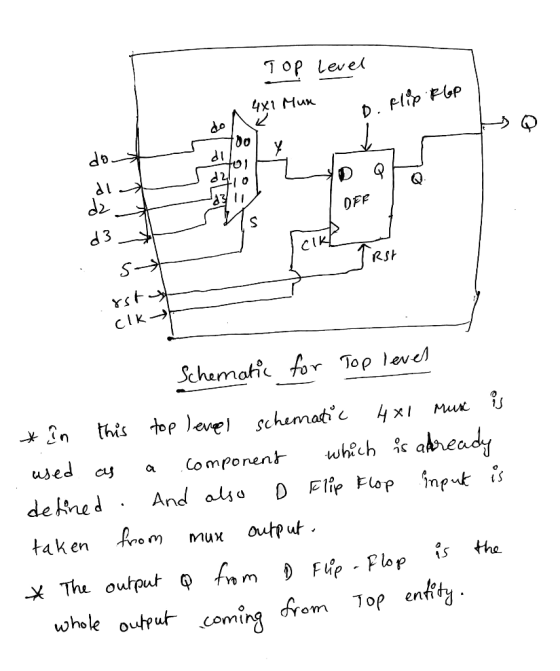
2) VHDL CODE for 4x1 Mux using as an component in another top level entity
-- 4x1 mux code
library IEEE;
use IEEE.std_logic_1164.all;
entity mux4 is
port(d0,d1,d2,d3: in STD_LOGIC;
x : in STD_LOGIC_VECTOR(1 downto 0);
y : out STD_LOGIC
);
end entity;
architecture synth of mux4 is
begin
with x select y <=
d0 when "00",
d1 when "01",
d2 when "10",
d3 when others;
end;
-- Top Level Entity
-- In this top level entity we are using given 4x1 mux as a
component
-- And giving it to D- Flip Flop input .
library IEEE;
use IEEE.std_logic_1164.all;
entity top is
port(rst,clk,d0,d1,d2,d3: in STD_LOGIC;
x : in STD_LOGIC_VECTOR(1 downto 0);
Q : out STD_LOGIC
);
end entity;
architecture behavioral of top is
component mux4 is
port(d0,d1,d2,d3: in STD_LOGIC;
x : in STD_LOGIC_VECTOR(1 downto 0);
y : out STD_LOGIC);
end component;
signal y: STD_LOGIC;
begin
mux4x1: mux4 port map ( d0 => d0,
d1 => d1,
d2 => d2,
d3 => d3,
x => x,
y => y );
-- D flip flop process - Sequential Block
top_seq: process(clk)
begin
if(rst) then
Q <= '0';
elsif rising_edge(clk) then
Q <= y;
end if;
end process;
end behavioral;
-- Testbench for TOP level block
library IEEE;
use IEEE.Std_logic_1164.all;
use IEEE.Numeric_Std.all;
entity top_tb is
end;
architecture testbench of top_tb is
component top
port(rst,clk,d0,d1,d2,d3: in STD_LOGIC;
x : in STD_LOGIC_VECTOR(1 downto 0);
Q : out STD_LOGIC
);
end component;
signal rst,clk,d0,d1,d2,d3: STD_LOGIC;
signal x: STD_LOGIC_VECTOR(1 downto 0);
signal Q: STD_LOGIC ;
constant clock_period: time := 10 ns;
signal stop_the_clock: boolean;
begin
uut: top port map ( rst => rst,
clk => clk,
d0 => d0,
d1 => d1,
d2 => d2,
d3 => d3,
x => x,
Q => Q );
stimulus: process
begin
rst <= '1';
d0 <= '0';
d1 <= '1';
d2 <= '0';
d3 <= '1';
x <= "00"; wait for 10 ns;
rst <= '0'; wait for 10 ns;
x <= "00"; wait for 10 ns;
x <= "01"; wait for 10 ns;
x <= "10"; wait for 10 ns;
x <= "11"; wait for 10 ns;
stop_the_clock <= true;
wait;
end process;
clocking: process
begin
while not stop_the_clock loop
clk <= '0', '1' after clock_period / 2;
wait for clock_period;
end loop;
wait;
end process;
end;
--Simulation Waveform

Add Answer to:
(20 pts)VHDL. Implement the logic circuit specified in the following truth table by using a 4:1 m...
Write a VHDL code using processes for the following logic circuit which include a shift register...
 Write a VHDL code using processes for the following logic
circuit which include a shift register and 4x1 multiplexer. Use the
entity below.
entity registers_min_max is
port( din : in std_logic_vector(3 downto 0);
reset : in std_logic;
clk : in
std_logic;
sel : in
std_logic_vector(1 downto 0);
reg_out : out std_logic_vector(3
downto 0));
end registers_min_max;
din reset RO clk reset R1 A C clk reset R2 clk reset R3 clk 3 0 sel LE
Write a VHDL code using processes for the following logic
circuit which include a shift register and 4x1 multiplexer. Use the
entity below.
entity registers_min_max is
port( din : in std_logic_vector(3 downto 0);
reset : in std_logic;
clk : in
std_logic;
sel : in
std_logic_vector(1 downto 0);
reg_out : out std_logic_vector(3
downto 0));
end registers_min_max;
din reset RO clk reset R1 A C clk reset R2 clk reset R3 clk 3 0 sel LE
Name: ·5. (10 lts) Find and correct errors in the following VHDL ed. IEEE ; library use IEEE . STD LOGIC-1104 . all...
 Name: ·5. (10 lts) Find and correct errors in the following VHDL ed. IEEE ; library use IEEE . STD LOGIC-1104 . all; entity cicuitl is port (a, b, elk: in STD_LOGIC: This part of the code its correct.That is, the entity definition and the 1ibraries are written correctly S out STD LOGIC) ond; architecture synth of eicuiti is begin This part of the code ธhould be a process that groups input a and input b together to forn a...
QUESTION 1 Complete the following peice of VHDL code with the necessary VHDL statements for a...
 QUESTION 1 Complete the following peice of VHDL code with the necessary VHDL statements for a counter that counts through this sequence(0,9,17,15,4,26) repeatedly. library IEEE use IEEE.STD_LOGIC_1164 ALL entity GCC is Port ( systemClock, reset in STD_LOGIC end GCC architecture Behavioral of GCC is stateOutput out STD LOGIC_ VECTOR (4 downto 0)) component FreqDivider is Port (systemClock in STD_LOGIC; slowClock: out STD LOGIC); end component, signal nextState, presentState: std_logic_vector(5 downto 0) := "00000"; signal slowClock: std_logic begin FD0: FreqDivider port...
I am making a 4-bit universal shift register that can perform right shift, left shift, and...
 I am making a 4-bit universal shift register that can perform
right shift, left shift, and parallel loading using 4-to-1
multiplexers in VHDL. I keep getting red lines for u3, u2, u1, u0.
The error says the following below. What is wrong with my code? How
can I fix it?
librarviees, use ieee.std_logic_1164.all; entity uni shift.reg.is porti 1 : in std. Jogis vector (3 downto.0); I, w, clock : in std logici 9: buffer std. Jogis vector (3 downto 0));...
I am making a 4-bit universal shift register that can perform
right shift, left shift, and parallel loading using 4-to-1
multiplexers in VHDL. I keep getting red lines for u3, u2, u1, u0.
The error says the following below. What is wrong with my code? How
can I fix it?
librarviees, use ieee.std_logic_1164.all; entity uni shift.reg.is porti 1 : in std. Jogis vector (3 downto.0); I, w, clock : in std logici 9: buffer std. Jogis vector (3 downto 0));...
3. Study the VHDL code below for the multiplexer: -mux.vhd library ieee; use ieee.std_logic_1164.all; use ieee.std_logic_unsigned.all;...
 3. Study the VHDL code below for the multiplexer: -mux.vhd library ieee; use ieee.std_logic_1164.all; use ieee.std_logic_unsigned.all; use jeee.std logic.arith.all; entity mux is port DIFF1, DIFF2: n std_logic_vector(4 downto O); ABSLT: out std_logic_vector(4 downto 0); CO: in std logic ); end mux; architecture behv of mux is begin with CO select ABSLT DIFF1 when o, a CO-0 selects B-A DIFF2 when 1',a Co-1 selects A-B "ZZZZZ" when others·.. high impedance otherwise end behy
Digital logic design Question 2 [4+6=10Marks] I. Implement following function using 16 x 1 multiplexer? F(A,B,C,D)...
 Digital logic design
Question 2 [4+6=10Marks] I. Implement following function using 16 x 1 multiplexer? F(A,B,C,D) = I l.ec.(D1, D2, D3, D4,10,11,13,15) II. Implement function F given above using 8 x 1 multiplexer?
Digital logic design
Question 2 [4+6=10Marks] I. Implement following function using 16 x 1 multiplexer? F(A,B,C,D) = I l.ec.(D1, D2, D3, D4,10,11,13,15) II. Implement function F given above using 8 x 1 multiplexer?
(a) The truth table below shows a certain function F(P,Q,R,S). Implement the function F using an 8:1 multiplexer, withou...
 (a) The truth table below shows a certain function
F(P,Q,R,S).
Implement the function F using an 8:1 multiplexer, without any
other logic gate. Only the constants 0 and 1, and the literals (but
not their complements) are available.
Fill in the inputs in the multiplexer diagram.
(b). Implement the function F
using a 24 decoder and a 4:1 multiplexer, and at most one logic
gate. Only the constants 0 and 1, and the literals (but not their
complements) are available....
(a) The truth table below shows a certain function
F(P,Q,R,S).
Implement the function F using an 8:1 multiplexer, without any
other logic gate. Only the constants 0 and 1, and the literals (but
not their complements) are available.
Fill in the inputs in the multiplexer diagram.
(b). Implement the function F
using a 24 decoder and a 4:1 multiplexer, and at most one logic
gate. Only the constants 0 and 1, and the literals (but not their
complements) are available....
8.(5 points).There is an error in following VHDL code. Find the error and correct (only that...
 8.(5 points).There is an error in following VHDL code. Find the error and correct (only that line of code). LIBRARY ieee; USE ieee.std_logic_1164.all; ENTITY dec2to4 IS PORT (i IN STD LOGIC VECTOR (1 DOWNTO 0); : En IN STD_LOGIC; d OUT STD LOGIC); END dec2to4; ARCHITECTURE dataflow OF dec2to4 IS BEGIN SIGNAL Eni: STD_LOGIC_VECTOR(2 DOWNTO 0); Eni <= En & i; -concatenate signals WITH Eni SELECT d <"0001" WHEN "100" "0010" WHEN "101", "0100" WHEN "110", "1000" WHEN "111", 0000"...
Please Write it in VHDL and complete the following code Create an entity called "regs" where...
 Please Write it in VHDL and complete the following code
Create an entity called "regs" where you infer a true dual port (both ports can independently either read or write to any location) memory consisting of 32 16-bit words (64 Bytes). It should have the following black box interface and behavior: entity regs is port clk, en, rst in std_logic; İdl, İd2 : in std logic vector (4 downto 0); __ Addresses wr_enl, wr_ en2 in std logic dinl, din2...
Please Write it in VHDL and complete the following code
Create an entity called "regs" where you infer a true dual port (both ports can independently either read or write to any location) memory consisting of 32 16-bit words (64 Bytes). It should have the following black box interface and behavior: entity regs is port clk, en, rst in std_logic; İdl, İd2 : in std logic vector (4 downto 0); __ Addresses wr_enl, wr_ en2 in std logic dinl, din2...
2. (a) Name and give a short description of the four design styles for describing a logic functio...
 2. (a) Name and give a short description of the four design styles for describing a logic function in an architecture? (b) List three concurrent signal assignment statements (c) The following two VHDL codes (architecture part) desanbe the logic diagram shown in Fig 1 (c) using different design styles. Discuss in detail the design style used for each description. begin My-Proc process (DOD 02 architecture architecture 1 of Entity 1 is Signal or out:std logie begin begin (IDO or D1...
 Write a VHDL code using processes for the following logic
circuit which include a shift register and 4x1 multiplexer. Use the
entity below.
entity registers_min_max is
port( din : in std_logic_vector(3 downto 0);
reset : in std_logic;
clk : in
std_logic;
sel : in
std_logic_vector(1 downto 0);
reg_out : out std_logic_vector(3
downto 0));
end registers_min_max;
din reset RO clk reset R1 A C clk reset R2 clk reset R3 clk 3 0 sel LE
Write a VHDL code using processes for the following logic
circuit which include a shift register and 4x1 multiplexer. Use the
entity below.
entity registers_min_max is
port( din : in std_logic_vector(3 downto 0);
reset : in std_logic;
clk : in
std_logic;
sel : in
std_logic_vector(1 downto 0);
reg_out : out std_logic_vector(3
downto 0));
end registers_min_max;
din reset RO clk reset R1 A C clk reset R2 clk reset R3 clk 3 0 sel LE
 Name: ·5. (10 lts) Find and correct errors in the following VHDL ed. IEEE ; library use IEEE . STD LOGIC-1104 . all; entity cicuitl is port (a, b, elk: in STD_LOGIC: This part of the code its correct.That is, the entity definition and the 1ibraries are written correctly S out STD LOGIC) ond; architecture synth of eicuiti is begin This part of the code ธhould be a process that groups input a and input b together to forn a...
 QUESTION 1 Complete the following peice of VHDL code with the necessary VHDL statements for a counter that counts through this sequence(0,9,17,15,4,26) repeatedly. library IEEE use IEEE.STD_LOGIC_1164 ALL entity GCC is Port ( systemClock, reset in STD_LOGIC end GCC architecture Behavioral of GCC is stateOutput out STD LOGIC_ VECTOR (4 downto 0)) component FreqDivider is Port (systemClock in STD_LOGIC; slowClock: out STD LOGIC); end component, signal nextState, presentState: std_logic_vector(5 downto 0) := "00000"; signal slowClock: std_logic begin FD0: FreqDivider port...
 I am making a 4-bit universal shift register that can perform
right shift, left shift, and parallel loading using 4-to-1
multiplexers in VHDL. I keep getting red lines for u3, u2, u1, u0.
The error says the following below. What is wrong with my code? How
can I fix it?
librarviees, use ieee.std_logic_1164.all; entity uni shift.reg.is porti 1 : in std. Jogis vector (3 downto.0); I, w, clock : in std logici 9: buffer std. Jogis vector (3 downto 0));...
I am making a 4-bit universal shift register that can perform
right shift, left shift, and parallel loading using 4-to-1
multiplexers in VHDL. I keep getting red lines for u3, u2, u1, u0.
The error says the following below. What is wrong with my code? How
can I fix it?
librarviees, use ieee.std_logic_1164.all; entity uni shift.reg.is porti 1 : in std. Jogis vector (3 downto.0); I, w, clock : in std logici 9: buffer std. Jogis vector (3 downto 0));...
 3. Study the VHDL code below for the multiplexer: -mux.vhd library ieee; use ieee.std_logic_1164.all; use ieee.std_logic_unsigned.all; use jeee.std logic.arith.all; entity mux is port DIFF1, DIFF2: n std_logic_vector(4 downto O); ABSLT: out std_logic_vector(4 downto 0); CO: in std logic ); end mux; architecture behv of mux is begin with CO select ABSLT DIFF1 when o, a CO-0 selects B-A DIFF2 when 1',a Co-1 selects A-B "ZZZZZ" when others·.. high impedance otherwise end behy
 Digital logic design
Question 2 [4+6=10Marks] I. Implement following function using 16 x 1 multiplexer? F(A,B,C,D) = I l.ec.(D1, D2, D3, D4,10,11,13,15) II. Implement function F given above using 8 x 1 multiplexer?
Digital logic design
Question 2 [4+6=10Marks] I. Implement following function using 16 x 1 multiplexer? F(A,B,C,D) = I l.ec.(D1, D2, D3, D4,10,11,13,15) II. Implement function F given above using 8 x 1 multiplexer?
 (a) The truth table below shows a certain function
F(P,Q,R,S).
Implement the function F using an 8:1 multiplexer, without any
other logic gate. Only the constants 0 and 1, and the literals (but
not their complements) are available.
Fill in the inputs in the multiplexer diagram.
(b). Implement the function F
using a 24 decoder and a 4:1 multiplexer, and at most one logic
gate. Only the constants 0 and 1, and the literals (but not their
complements) are available....
(a) The truth table below shows a certain function
F(P,Q,R,S).
Implement the function F using an 8:1 multiplexer, without any
other logic gate. Only the constants 0 and 1, and the literals (but
not their complements) are available.
Fill in the inputs in the multiplexer diagram.
(b). Implement the function F
using a 24 decoder and a 4:1 multiplexer, and at most one logic
gate. Only the constants 0 and 1, and the literals (but not their
complements) are available....
 8.(5 points).There is an error in following VHDL code. Find the error and correct (only that line of code). LIBRARY ieee; USE ieee.std_logic_1164.all; ENTITY dec2to4 IS PORT (i IN STD LOGIC VECTOR (1 DOWNTO 0); : En IN STD_LOGIC; d OUT STD LOGIC); END dec2to4; ARCHITECTURE dataflow OF dec2to4 IS BEGIN SIGNAL Eni: STD_LOGIC_VECTOR(2 DOWNTO 0); Eni <= En & i; -concatenate signals WITH Eni SELECT d <"0001" WHEN "100" "0010" WHEN "101", "0100" WHEN "110", "1000" WHEN "111", 0000"...
 Please Write it in VHDL and complete the following code
Create an entity called "regs" where you infer a true dual port (both ports can independently either read or write to any location) memory consisting of 32 16-bit words (64 Bytes). It should have the following black box interface and behavior: entity regs is port clk, en, rst in std_logic; İdl, İd2 : in std logic vector (4 downto 0); __ Addresses wr_enl, wr_ en2 in std logic dinl, din2...
Please Write it in VHDL and complete the following code
Create an entity called "regs" where you infer a true dual port (both ports can independently either read or write to any location) memory consisting of 32 16-bit words (64 Bytes). It should have the following black box interface and behavior: entity regs is port clk, en, rst in std_logic; İdl, İd2 : in std logic vector (4 downto 0); __ Addresses wr_enl, wr_ en2 in std logic dinl, din2...
 2. (a) Name and give a short description of the four design styles for describing a logic function in an architecture? (b) List three concurrent signal assignment statements (c) The following two VHDL codes (architecture part) desanbe the logic diagram shown in Fig 1 (c) using different design styles. Discuss in detail the design style used for each description. begin My-Proc process (DOD 02 architecture architecture 1 of Entity 1 is Signal or out:std logie begin begin (IDO or D1...
Most questions answered within 3 hours.
-
Where is the error in this code sequence?
String s1 = "Hello";
String s2 = "ello";...
asked 11 months ago -
Financial data for Joel de Paris, Inc., for last year
follow:
Joel de Paris, Inc.
Balance...
asked 11 months ago -
Consider this reaction:
Al2(SO4)3 (aq)+ BaCl3
(aq) Al2Cl6 (aq)- +
3BaSO4(s) . What is the...
asked 11 months ago -
Suppose that Savneet is considering increasing her
recent random sample from 20 car rentals to 40...
asked 11 months ago -
Trucks arrive at an unloading terminal at an average rate of 120
per hour.
Trucks arrive...
asked 11 months ago -
Why are methanol and ethanol completely soluble in water while
octanol is not very little soluble....
asked 11 months ago -
A facilities manager at a university reads in a research report
that the mean amount of...
asked 11 months ago -
When the CuSO4 is rehydrated by adding water to the anhydrous
compound, is this an endothermic...
asked 11 months ago -
A ray of sunlight is passing from diamond into crown glass; the
angle of incidence is...
asked 11 months ago -
A block of mass 0.249 kg is placed on top of a light, vertical
spring of...
asked 11 months ago -
how do the kidneys compensate in the presences of acidosis
a) trigger hyperventilate
b) reserve acid...
asked 11 months ago -
Question 501 pts
The rental rate of capital to the firm increases. Which of the
following...
asked 11 months ago