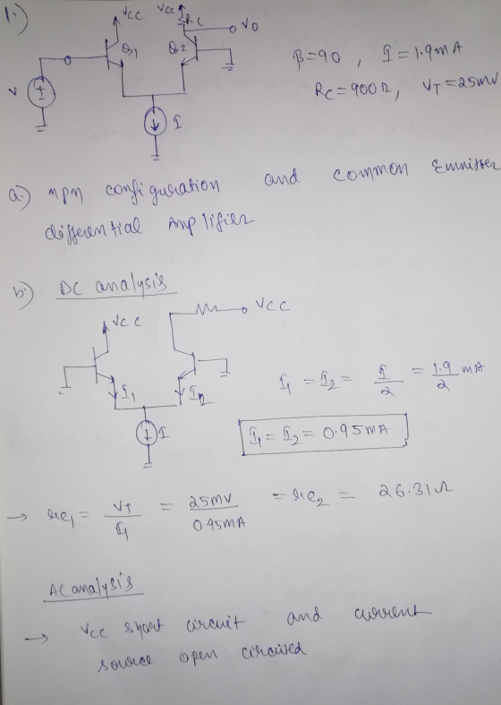
The BJTs in the circuit below has the same β = 90 and the same collector current. Assume I = 1.9 mA, RC=900 Ω, and use VT = 25 mV.
a- What is the configuration of each stage of the amplifier? Explain and add to the figure below the input and the output of each stage.
b- Draw the small signal equivalent circuit and find the small signal parameters.
c- Find the voltage gain of this amplifier

Homework Answers

Add Answer to:
The BJTs in the circuit below has the same β = 90 and the same
collector...
The BJT amplifier circuit in the figure below has β = 90. Use VT = 25...
 The BJT amplifier circuit in the figure below has β = 90. Use VT
= 25 mV
a- Draw the DC equivalent circuit and calculate IC.
b- Draw the small signal equivalent circuit and calculate the
small signal parameters.
c- Find the voltage gain
+9V 3 kΩ C2 = 1 uF HE C = 1uF + υο 10 kΩ Cz = 50 uF - . υ 9 kΩ Η. 6. ΚΩ -9 V
The BJT amplifier circuit in the figure below has β = 90. Use VT
= 25 mV
a- Draw the DC equivalent circuit and calculate IC.
b- Draw the small signal equivalent circuit and calculate the
small signal parameters.
c- Find the voltage gain
+9V 3 kΩ C2 = 1 uF HE C = 1uF + υο 10 kΩ Cz = 50 uF - . υ 9 kΩ Η. 6. ΚΩ -9 V
For the circuit shown below, let Vcc 9 V R2 RE-0.11 kQ, R1 3.6 k2. and R2 -5.6 kQ. The transistor parameters are β-200, VBE(on)-OTV, VA-100 V and VT = 0.026 V. (a) Determine the quiescent value o...
 For the circuit shown below, let Vcc 9 V R2 RE-0.11 kQ, R1 3.6 k2. and R2 -5.6 kQ. The transistor parameters are β-200, VBE(on)-OTV, VA-100 V and VT = 0.026 V. (a) Determine the quiescent value of IEQ (b) Find the small-signal voltage gain Av Vo/vs (c) Determine the output resistance R, looking into output terminals Av= 0.5589 Ro-0.4688 Ω Ro-0.9118 Ω leQ- 23.76 mA Ra " 0.6538 Ω leo 39.52 mA A, 0.9938
For the circuit shown below,...
For the circuit shown below, let Vcc 9 V R2 RE-0.11 kQ, R1 3.6 k2. and R2 -5.6 kQ. The transistor parameters are β-200, VBE(on)-OTV, VA-100 V and VT = 0.026 V. (a) Determine the quiescent value of IEQ (b) Find the small-signal voltage gain Av Vo/vs (c) Determine the output resistance R, looking into output terminals Av= 0.5589 Ro-0.4688 Ω Ro-0.9118 Ω leQ- 23.76 mA Ra " 0.6538 Ω leo 39.52 mA A, 0.9938
For the circuit shown below,...
can you do 4.83 Ar- Q Sea 100 V, what does the gain become? age at...
 can
you do 4.83
Ar- Q Sea 100 V, what does the gain become? age at the collector. (b) Replacing the transistor by its T model, da the small-signal equivalent circuit of the a plifier. Analyze the resulting circuit to dete mine the voltage gain t/ 04.81 Consider the CE amplifier circuit of Fig. 4.43(a). It is required to design the circuit (i.e., find values for I and Rc) to meet the following specifications: (a) R,5kn (b) the voltage gain...
can
you do 4.83
Ar- Q Sea 100 V, what does the gain become? age at the collector. (b) Replacing the transistor by its T model, da the small-signal equivalent circuit of the a plifier. Analyze the resulting circuit to dete mine the voltage gain t/ 04.81 Consider the CE amplifier circuit of Fig. 4.43(a). It is required to design the circuit (i.e., find values for I and Rc) to meet the following specifications: (a) R,5kn (b) the voltage gain...
The 1 mA. V, ls -VE -15 15 V, in the following differential amplifier circuit, Vcc parameters are given as β, 100, VBE# 0.7 V, pr-25 mV, K.-100 V. transistor Rc-10 kΩ For: RE-150 Ω Rc Rc REE-200...
 The 1 mA. V, ls -VE -15 15 V, in the following differential amplifier circuit, Vcc parameters are given as β, 100, VBE# 0.7 V, pr-25 mV, K.-100 V. transistor Rc-10 kΩ For: RE-150 Ω Rc Rc REE-200 kΩ a) What is the input differential resistance, Rid b) What is the overall voltage gain vV? You c) What is input common mode resistance, d) What is the worst case common mode gain that appear across the two input terminals? (4...
Please answer clearly 2. Consider the circuit shown in Figure 1. Determine values of Ri, R2, and Rc to provide the quie...
 Please answer clearly
2. Consider the circuit shown in Figure 1. Determine values of Ri, R2, and Rc to provide the quiescent emitter current 1.5 mA and the quiescent collector to emitter voltage 5V. Assume β 100, Re-I㏀、Va= 200V, VBEon-0.7V, and VT= 25mV. R1 Rc Vcc に 10v R2 Re Figure 1: BJT biasing configuration
2. Consider the circuit shown in Figure 1. Determine values of Ri, R2, and Rc to provide the quiescent emitter current 1.5 mA and the...
Please answer clearly
2. Consider the circuit shown in Figure 1. Determine values of Ri, R2, and Rc to provide the quiescent emitter current 1.5 mA and the quiescent collector to emitter voltage 5V. Assume β 100, Re-I㏀、Va= 200V, VBEon-0.7V, and VT= 25mV. R1 Rc Vcc に 10v R2 Re Figure 1: BJT biasing configuration
2. Consider the circuit shown in Figure 1. Determine values of Ri, R2, and Rc to provide the quiescent emitter current 1.5 mA and the...
All transistors in the circuit below are identical. Transistor parameters are hFE=hfe=β= 200, IS=10 fA and...
 All transistors in the circuit below are identical. Transistor
parameters are hFE=hfe=β= 200,
IS=10 fA and VT = 26 mV.
a. Obtain the differential mode gain equation:
Add=(V01-V02)/(V1-V2).
b. VDD=5V, -VSS=-5V, IB=2mA,
RC=2kΩ and RL=3kΩ. Calculate the differential
mode gain (Add) of the circuit.
c. How do you connect a common emitter stage to one of the outputs
of the circuit? Please draw on the circuit.
+VDD Rc 3 Rc Voi VO2 w R Vi V2 IB -Vss
All transistors in the circuit below are identical. Transistor
parameters are hFE=hfe=β= 200,
IS=10 fA and VT = 26 mV.
a. Obtain the differential mode gain equation:
Add=(V01-V02)/(V1-V2).
b. VDD=5V, -VSS=-5V, IB=2mA,
RC=2kΩ and RL=3kΩ. Calculate the differential
mode gain (Add) of the circuit.
c. How do you connect a common emitter stage to one of the outputs
of the circuit? Please draw on the circuit.
+VDD Rc 3 Rc Voi VO2 w R Vi V2 IB -Vss
In the circuit of given below, Vsig is a small sine wave signal with zero average. The transistor...
 In the circuit of given below, Vsig is a small sine wave signal with zero average. The transistor B is 100. a) Find the value of RE to establish a dc emitter current of about 0.5 mA. b) Find Rc to establish a dc collector voltage of about +5 V c) For RL10 kS2 and the transistor ro 200 k2, draw the small-signal equivalent circuit 5. of the amplifier and determine its overall voltage gain +15 V Re O Vo...
1. Problem 1: For the circuit below, where β-100 and VT 25mV a. Find the dc...
 1. Problem 1: For the circuit below, where β-100 and VT 25mV a. Find the dc collector current, Ic. b. Find the small signal parameters: gm , Γπ and re- c. Draw the small-signal equivalent circuit by replacing the BJT with its hybrid-t model. d. Draw the small-signal equivalent circuit by replacing the BJT with its T model. e. Use the circuit in c or d to determine the voltage gains (Ao, A.) and overall gain (Gv) 5V 1V Vout...
QUESTION5 The small-signal ac equivalent cireuit of a transistor amplifier with collector feedback is shown in...
 QUESTION5 The small-signal ac equivalent cireuit of a transistor amplifier with collector feedback is shown in the figure below. Assume the following circuit values: B- 200, re" i i o. RF-180 kn. Rc" 2.7 ?, RO-3.3 ?, ??-?2 = 10 ?? If the input voltage Vi-5 co (90 t) mv. determine the magnitude of the steady-state ac output voltage Vo (in mV), across the output load resistor Ro. Hint: Use node analysis to find the output node voltage, and note...
3) BJT Gain Stage 1 mA BJT Parameters β 100 nVr-30 mV 5V Vo 6meg c,,-8 pF Vi 500 27u Vs VB is an ...
 3) BJT Gain Stage 1 mA BJT Parameters β 100 nVr-30 mV 5V Vo 6meg c,,-8 pF Vi 500 27u Vs VB is an ideal dc voltage source a) What type of gain stage is realized by this BJT amplifier? b) Find a value for the input resistance Ri seen at node Vi. c) Find a value for the mid-band voltage gain Av-Vo/Vs. d) Determine the upper corner frequency fp2 imposed by the parasitic caps of the BJT
3) BJT...
3) BJT Gain Stage 1 mA BJT Parameters β 100 nVr-30 mV 5V Vo 6meg c,,-8 pF Vi 500 27u Vs VB is an ideal dc voltage source a) What type of gain stage is realized by this BJT amplifier? b) Find a value for the input resistance Ri seen at node Vi. c) Find a value for the mid-band voltage gain Av-Vo/Vs. d) Determine the upper corner frequency fp2 imposed by the parasitic caps of the BJT
3) BJT...
 The BJT amplifier circuit in the figure below has β = 90. Use VT
= 25 mV
a- Draw the DC equivalent circuit and calculate IC.
b- Draw the small signal equivalent circuit and calculate the
small signal parameters.
c- Find the voltage gain
+9V 3 kΩ C2 = 1 uF HE C = 1uF + υο 10 kΩ Cz = 50 uF - . υ 9 kΩ Η. 6. ΚΩ -9 V
The BJT amplifier circuit in the figure below has β = 90. Use VT
= 25 mV
a- Draw the DC equivalent circuit and calculate IC.
b- Draw the small signal equivalent circuit and calculate the
small signal parameters.
c- Find the voltage gain
+9V 3 kΩ C2 = 1 uF HE C = 1uF + υο 10 kΩ Cz = 50 uF - . υ 9 kΩ Η. 6. ΚΩ -9 V
 For the circuit shown below, let Vcc 9 V R2 RE-0.11 kQ, R1 3.6 k2. and R2 -5.6 kQ. The transistor parameters are β-200, VBE(on)-OTV, VA-100 V and VT = 0.026 V. (a) Determine the quiescent value of IEQ (b) Find the small-signal voltage gain Av Vo/vs (c) Determine the output resistance R, looking into output terminals Av= 0.5589 Ro-0.4688 Ω Ro-0.9118 Ω leQ- 23.76 mA Ra " 0.6538 Ω leo 39.52 mA A, 0.9938
For the circuit shown below,...
For the circuit shown below, let Vcc 9 V R2 RE-0.11 kQ, R1 3.6 k2. and R2 -5.6 kQ. The transistor parameters are β-200, VBE(on)-OTV, VA-100 V and VT = 0.026 V. (a) Determine the quiescent value of IEQ (b) Find the small-signal voltage gain Av Vo/vs (c) Determine the output resistance R, looking into output terminals Av= 0.5589 Ro-0.4688 Ω Ro-0.9118 Ω leQ- 23.76 mA Ra " 0.6538 Ω leo 39.52 mA A, 0.9938
For the circuit shown below,...
 can
you do 4.83
Ar- Q Sea 100 V, what does the gain become? age at the collector. (b) Replacing the transistor by its T model, da the small-signal equivalent circuit of the a plifier. Analyze the resulting circuit to dete mine the voltage gain t/ 04.81 Consider the CE amplifier circuit of Fig. 4.43(a). It is required to design the circuit (i.e., find values for I and Rc) to meet the following specifications: (a) R,5kn (b) the voltage gain...
can
you do 4.83
Ar- Q Sea 100 V, what does the gain become? age at the collector. (b) Replacing the transistor by its T model, da the small-signal equivalent circuit of the a plifier. Analyze the resulting circuit to dete mine the voltage gain t/ 04.81 Consider the CE amplifier circuit of Fig. 4.43(a). It is required to design the circuit (i.e., find values for I and Rc) to meet the following specifications: (a) R,5kn (b) the voltage gain...
 The 1 mA. V, ls -VE -15 15 V, in the following differential amplifier circuit, Vcc parameters are given as β, 100, VBE# 0.7 V, pr-25 mV, K.-100 V. transistor Rc-10 kΩ For: RE-150 Ω Rc Rc REE-200 kΩ a) What is the input differential resistance, Rid b) What is the overall voltage gain vV? You c) What is input common mode resistance, d) What is the worst case common mode gain that appear across the two input terminals? (4...
 Please answer clearly
2. Consider the circuit shown in Figure 1. Determine values of Ri, R2, and Rc to provide the quiescent emitter current 1.5 mA and the quiescent collector to emitter voltage 5V. Assume β 100, Re-I㏀、Va= 200V, VBEon-0.7V, and VT= 25mV. R1 Rc Vcc に 10v R2 Re Figure 1: BJT biasing configuration
2. Consider the circuit shown in Figure 1. Determine values of Ri, R2, and Rc to provide the quiescent emitter current 1.5 mA and the...
Please answer clearly
2. Consider the circuit shown in Figure 1. Determine values of Ri, R2, and Rc to provide the quiescent emitter current 1.5 mA and the quiescent collector to emitter voltage 5V. Assume β 100, Re-I㏀、Va= 200V, VBEon-0.7V, and VT= 25mV. R1 Rc Vcc に 10v R2 Re Figure 1: BJT biasing configuration
2. Consider the circuit shown in Figure 1. Determine values of Ri, R2, and Rc to provide the quiescent emitter current 1.5 mA and the...
 All transistors in the circuit below are identical. Transistor
parameters are hFE=hfe=β= 200,
IS=10 fA and VT = 26 mV.
a. Obtain the differential mode gain equation:
Add=(V01-V02)/(V1-V2).
b. VDD=5V, -VSS=-5V, IB=2mA,
RC=2kΩ and RL=3kΩ. Calculate the differential
mode gain (Add) of the circuit.
c. How do you connect a common emitter stage to one of the outputs
of the circuit? Please draw on the circuit.
+VDD Rc 3 Rc Voi VO2 w R Vi V2 IB -Vss
All transistors in the circuit below are identical. Transistor
parameters are hFE=hfe=β= 200,
IS=10 fA and VT = 26 mV.
a. Obtain the differential mode gain equation:
Add=(V01-V02)/(V1-V2).
b. VDD=5V, -VSS=-5V, IB=2mA,
RC=2kΩ and RL=3kΩ. Calculate the differential
mode gain (Add) of the circuit.
c. How do you connect a common emitter stage to one of the outputs
of the circuit? Please draw on the circuit.
+VDD Rc 3 Rc Voi VO2 w R Vi V2 IB -Vss
 In the circuit of given below, Vsig is a small sine wave signal with zero average. The transistor B is 100. a) Find the value of RE to establish a dc emitter current of about 0.5 mA. b) Find Rc to establish a dc collector voltage of about +5 V c) For RL10 kS2 and the transistor ro 200 k2, draw the small-signal equivalent circuit 5. of the amplifier and determine its overall voltage gain +15 V Re O Vo...
 1. Problem 1: For the circuit below, where β-100 and VT 25mV a. Find the dc collector current, Ic. b. Find the small signal parameters: gm , Γπ and re- c. Draw the small-signal equivalent circuit by replacing the BJT with its hybrid-t model. d. Draw the small-signal equivalent circuit by replacing the BJT with its T model. e. Use the circuit in c or d to determine the voltage gains (Ao, A.) and overall gain (Gv) 5V 1V Vout...
 QUESTION5 The small-signal ac equivalent cireuit of a transistor amplifier with collector feedback is shown in the figure below. Assume the following circuit values: B- 200, re" i i o. RF-180 kn. Rc" 2.7 ?, RO-3.3 ?, ??-?2 = 10 ?? If the input voltage Vi-5 co (90 t) mv. determine the magnitude of the steady-state ac output voltage Vo (in mV), across the output load resistor Ro. Hint: Use node analysis to find the output node voltage, and note...
 3) BJT Gain Stage 1 mA BJT Parameters β 100 nVr-30 mV 5V Vo 6meg c,,-8 pF Vi 500 27u Vs VB is an ideal dc voltage source a) What type of gain stage is realized by this BJT amplifier? b) Find a value for the input resistance Ri seen at node Vi. c) Find a value for the mid-band voltage gain Av-Vo/Vs. d) Determine the upper corner frequency fp2 imposed by the parasitic caps of the BJT
3) BJT...
3) BJT Gain Stage 1 mA BJT Parameters β 100 nVr-30 mV 5V Vo 6meg c,,-8 pF Vi 500 27u Vs VB is an ideal dc voltage source a) What type of gain stage is realized by this BJT amplifier? b) Find a value for the input resistance Ri seen at node Vi. c) Find a value for the mid-band voltage gain Av-Vo/Vs. d) Determine the upper corner frequency fp2 imposed by the parasitic caps of the BJT
3) BJT...
Most questions answered within 3 hours.
-
Where is the error in this code sequence?
String s1 = "Hello";
String s2 = "ello";...
asked 10 months ago -
Financial data for Joel de Paris, Inc., for last year
follow:
Joel de Paris, Inc.
Balance...
asked 10 months ago -
Consider this reaction:
Al2(SO4)3 (aq)+ BaCl3
(aq) Al2Cl6 (aq)- +
3BaSO4(s) . What is the...
asked 10 months ago -
Suppose that Savneet is considering increasing her
recent random sample from 20 car rentals to 40...
asked 10 months ago -
Trucks arrive at an unloading terminal at an average rate of 120
per hour.
Trucks arrive...
asked 10 months ago -
Why are methanol and ethanol completely soluble in water while
octanol is not very little soluble....
asked 10 months ago -
A facilities manager at a university reads in a research report
that the mean amount of...
asked 10 months ago -
When the CuSO4 is rehydrated by adding water to the anhydrous
compound, is this an endothermic...
asked 10 months ago -
A ray of sunlight is passing from diamond into crown glass; the
angle of incidence is...
asked 10 months ago -
A block of mass 0.249 kg is placed on top of a light, vertical
spring of...
asked 10 months ago -
how do the kidneys compensate in the presences of acidosis
a) trigger hyperventilate
b) reserve acid...
asked 10 months ago -
Question 501 pts
The rental rate of capital to the firm increases. Which of the
following...
asked 10 months ago