
Homework Answers
Add Answer to:
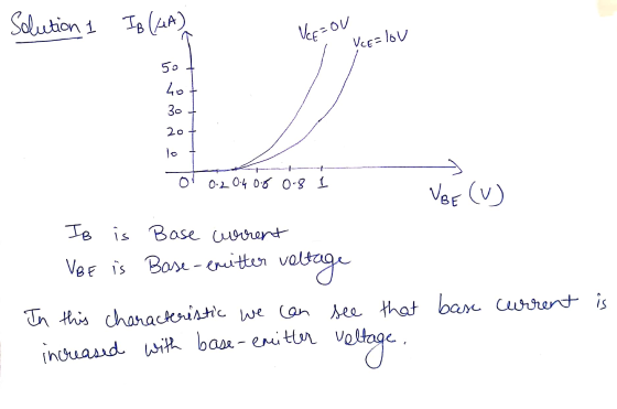
1) Plot base current of a npn transistor versus base-emitter voltage 2) Plot Gate current of...
1. a) Calculate the change in base emitter voltage if the collector current increase by 2...
1. a) Calculate the change in base emitter voltage if the collector current increase by 2 and by 10. b) A MOS transistor require a gate source overdrive voltage of 100mV for 100uA drain current. Calculate the change in gate to source voltage if the drain current increases by 2 and by 10. Compare it to problem a) and comment the results.
An NPN Transistor has a DC base bias voltage, Vb of 10.8v and an input base...
An NPN Transistor has a DC base bias voltage, Vb of 10.8v and an input base resistor, Rb of 80kΩ. What will be the value of the base current (in μA) into the transistor?
Consider a silicon device (which happens to be an npn bipolar transistor) with an emitter doping...
Consider a silicon device (which happens to be an npn bipolar transistor) with an emitter doping of 10^17/cm3, a base doping of 8x10^15/cm3 and a collector doping of 2x10^15/cm3. Carefully calculate how the band diagram, charge density, electric field and electrostatic potential as a function of distance for this device changes from the equilibrium case when this bipolar transistor is properly biased to work as an amplifier. In other words, show how the band diagram changes when the emitter-base junction...
2. (15 pts) An npn bipolar junction transistor is biased in the forward-active region. The common-base...
 2. (15 pts) An npn bipolar junction transistor is biased in the forward-active region. The common-base current gain, α 0.95. The input emitter current is IE-4.6 mA. a) Calculate the collector current Ic b) Calculate the common-emitter current gain, B c) Calculate the base current IB IB
2. Consider an N-channel MOSFET circuit where the gate and drain terminals are shorted to- gether...
 Please help, and explain as much as possible. Thank
you!
2. Consider an N-channel MOSFET circuit where the gate and drain terminals are shorted to- gether2 as shown in Figre 2. Assume that the MOSFET has trans-conductance parameter of gm = 0.5mA/V and the threshold voltage of 0.7V (a) Identify in which region the n-channel MOSFET is operating (Triode region or Saturation region)? (b) Write MATLAB code to compute the drain current for the following gate-to-source voltage, Vcs Ves-VDs 0,1,2,3,4,5,6,7...
Please help, and explain as much as possible. Thank
you!
2. Consider an N-channel MOSFET circuit where the gate and drain terminals are shorted to- gether2 as shown in Figre 2. Assume that the MOSFET has trans-conductance parameter of gm = 0.5mA/V and the threshold voltage of 0.7V (a) Identify in which region the n-channel MOSFET is operating (Triode region or Saturation region)? (b) Write MATLAB code to compute the drain current for the following gate-to-source voltage, Vcs Ves-VDs 0,1,2,3,4,5,6,7...
Problem 2. A silicon NPN bipolar transistor has the following specifications: Emitter: N+: ND =1018 cm-3...
Problem 2. A silicon NPN bipolar transistor has the following specifications: Emitter: N+: ND =1018 cm-3 , base: p-type, NA=1015 cm-3, collector: N-type, ND=5x1015 cm-3 . 1. Draw the energy band diagram of the transistor at thermal equilibrium, 2. If the transistor is biased at Normal Active Mode, emitter-base junction forward biased with 1 V, and collector-base junction is reverse biased with 4V, draw the energy band diagram.
QUESTION 1 For normal operation of an npn transistor, the base must be O a. disconnected...
 QUESTION 1 For normal operation of an npn transistor, the base must be O a. disconnected O b. negative with respect to the emitter O C positive with respect to the emitter O d. positive with respect to the collector QUESTION 2 The bias condition for a transistor to be used as a linear amplifier is called O a. forward-reverse b. forward-forward C. reverse-reverse d. collector bias
1.what is the relation between emitter current and collector current in the transistor. 2. what is...
1.what is the relation between emitter current and collector current in the transistor. 2. what is the relation between emitter ,collector and base current in th transistor ??
Consider an NMOS transistor with the gate connected to a voltage source, its source connected to...
Consider an NMOS transistor with the gate connected to a voltage source, its source connected to ground, bulk also connected to ground and the drain connected a variable voltage source. The NMOS transistor properties are k’ = 0.2mA/V2, ?= 0.025 V-1, W= 16?? and L = 1?? , Vto= 0.8V and gate oxide thickness of tox = 100Å. Assuming the transistor in saturation region and ignoring any Early effects, calculate the gate current, the gate source voltage and the gate...
1. An npn transistor is operating in the forward-active region with a base current of 3...
1. An npn transistor is operating in the forward-active region with a base current of 3 μA. It is found that IC = 225 μA for VCE = 5 V and IC = 265 μA for VCE = 10 V. What are the values of β and VA for this transistor
 2. (15 pts) An npn bipolar junction transistor is biased in the forward-active region. The common-base current gain, α 0.95. The input emitter current is IE-4.6 mA. a) Calculate the collector current Ic b) Calculate the common-emitter current gain, B c) Calculate the base current IB IB
 Please help, and explain as much as possible. Thank
you!
2. Consider an N-channel MOSFET circuit where the gate and drain terminals are shorted to- gether2 as shown in Figre 2. Assume that the MOSFET has trans-conductance parameter of gm = 0.5mA/V and the threshold voltage of 0.7V (a) Identify in which region the n-channel MOSFET is operating (Triode region or Saturation region)? (b) Write MATLAB code to compute the drain current for the following gate-to-source voltage, Vcs Ves-VDs 0,1,2,3,4,5,6,7...
Please help, and explain as much as possible. Thank
you!
2. Consider an N-channel MOSFET circuit where the gate and drain terminals are shorted to- gether2 as shown in Figre 2. Assume that the MOSFET has trans-conductance parameter of gm = 0.5mA/V and the threshold voltage of 0.7V (a) Identify in which region the n-channel MOSFET is operating (Triode region or Saturation region)? (b) Write MATLAB code to compute the drain current for the following gate-to-source voltage, Vcs Ves-VDs 0,1,2,3,4,5,6,7...
 QUESTION 1 For normal operation of an npn transistor, the base must be O a. disconnected O b. negative with respect to the emitter O C positive with respect to the emitter O d. positive with respect to the collector QUESTION 2 The bias condition for a transistor to be used as a linear amplifier is called O a. forward-reverse b. forward-forward C. reverse-reverse d. collector bias
Most questions answered within 3 hours.
-
Where is the error in this code sequence?
String s1 = "Hello";
String s2 = "ello";...
asked 11 months ago -
Financial data for Joel de Paris, Inc., for last year
follow:
Joel de Paris, Inc.
Balance...
asked 11 months ago -
Consider this reaction:
Al2(SO4)3 (aq)+ BaCl3
(aq) Al2Cl6 (aq)- +
3BaSO4(s) . What is the...
asked 11 months ago -
Suppose that Savneet is considering increasing her
recent random sample from 20 car rentals to 40...
asked 11 months ago -
Trucks arrive at an unloading terminal at an average rate of 120
per hour.
Trucks arrive...
asked 11 months ago -
Why are methanol and ethanol completely soluble in water while
octanol is not very little soluble....
asked 11 months ago -
A facilities manager at a university reads in a research report
that the mean amount of...
asked 11 months ago -
When the CuSO4 is rehydrated by adding water to the anhydrous
compound, is this an endothermic...
asked 11 months ago -
A ray of sunlight is passing from diamond into crown glass; the
angle of incidence is...
asked 11 months ago -
A block of mass 0.249 kg is placed on top of a light, vertical
spring of...
asked 11 months ago -
how do the kidneys compensate in the presences of acidosis
a) trigger hyperventilate
b) reserve acid...
asked 11 months ago -
Question 501 pts
The rental rate of capital to the firm increases. Which of the
following...
asked 11 months ago