Write structural/heirarcherical Verilog to design 8 to 1 MUX using 2 to 1 and 4 to...
Homework Answers
8 :1 multiplexer using 4:1 and 2:1 multiplexer Digital circuit diagram.
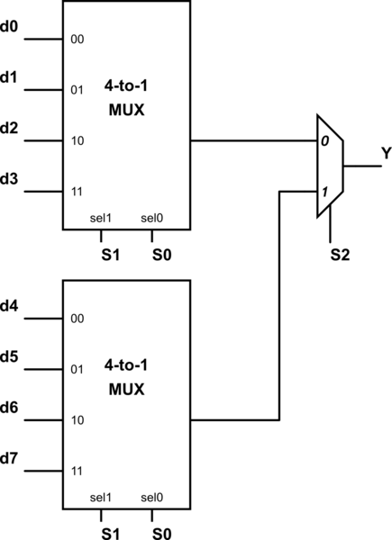
Truth Table:
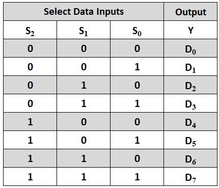
Verilog Code for 8 to 1 mux using two 4 to 1 mux and one 2 to 1 mux;
// 8to1 mux initialization for 4 bit per input
module mux_8x1(
input [3:0] a,
input [3:0] b,
input [3:0] c,
input [3:0] d,
input [3:0] e,
input [3:0] f,
input [3:0] g,
input [3:0] h,
input [2:0] sel,
output [3:0] out
);
wire [3:0] w1,w2,w3,w4,w5;
mux mx1[3:0](a,b,c,d,sel[1:0],w1);
mux mx2[3:0](e,f,g,h,sel[1:0],w2);
not n1[3:0](w3,sel[2]);
and a1[3:0](w4,w1,w3);
and a2[3:0](w5,w2,sel[2]);
or o1[3:0](out,w4,w5);
endmodule
module mux(in1,in2,in3,in4,select,op);
input [3:0] in1;
input [3:0] in2;
input [3:0] in3;
input [3:0] in4;
input [1:0] select;
output reg [3:0] op;
always@(in1 or in2 or in3 or in4 or select) begin
case (select)
2'b00 : op <= in1;
2'b01 : op <= in2;
2'b10 : op <= in3;
2'b11 : op <= in4;
endcase
end
endmodule
//testench
module tb_8to1_mux;
reg [3:0] a;
reg [3:0] b;
reg [3:0] c;
reg [3:0] d;
reg [3:0] e;
reg [3:0] f;
reg [3:0] g;
reg [3:0] h;
reg [2:0] sel;
wire [3:0] out;
integer i;
mux_8x1 mux0(.a(a),.b(b),.c(c),.d
(d),.e(e),.f(f),.g(g),.h(h),.sel(sel),.out(out));
initial begin
$dumpfile("muxx.vcd");
$dumpvars(0,tb_8to1_mux);
$monitor ("[%0t] sel=0x%0h a=0x%0h b=0x%0h c=0x%0h d=0x%0h e=0x%0h
f=0x%0h g=0x%0h h=0x%0h out=0x%0h", $time, sel, a, b, c, d, e, f,
g, h, out);
sel <= 0;
a <= $random;
b <= $random;
c <= $random;
d <= $random;
e <= $random;
f <= $random;
g <= $random;
h <= $random;
for (i = 0; i < 7; i=i+1) begin
#5 sel <= i;
end
#5 $finish;
end
endmodule
Add Answer to:
Write structural/heirarcherical Verilog to design 8 to 1 MUX using
2 to 1 and 4 to...
Design a 32-to1 multiplexer (MUX) using 1. 8-to-1 MUX and 2-to-4 decoders. 2. 4-to-1 MUX and...
Design a 32-to1 multiplexer (MUX) using 1. 8-to-1 MUX and 2-to-4 decoders. 2. 4-to-1 MUX and 2-to-4 decoders. Thank you!
a) Write a verilog module for 1:4 Demultiplexer using verilog primitives. b) Design 1-to-4 DEMUX using...
a) Write a verilog module for 1:4 Demultiplexer using verilog primitives. b) Design 1-to-4 DEMUX using tristate buffers in verilog. c) Write a code in NIOS-II assembly to execute following statement: b=(a+b)-(c+d)
Design an 8-bit full adder using Verilog (Use only 1-bit full adders). Write the design code,...
Design an 8-bit full adder using Verilog (Use only 1-bit full adders). Write the design code, test-bench code of it, and test your design with six inputs. Note: Only use Verilog to design 8-bit full adder.
Counter I. Using structural verilog, write a top-level module for the One's Counter with as many ...
 Counter I. Using structural verilog, write a top-level module for the One's Counter with as many instances of half adders and full adders as needed according to Prelab C.1 2. Write a test bench to verity the One's Counter design. Provide stimulus patterns in such a way that every input output of each half and full adder toggle (change value) at least once
Counter I. Using structural verilog, write a top-level module for the One's Counter with as many instances...
Counter I. Using structural verilog, write a top-level module for the One's Counter with as many instances of half adders and full adders as needed according to Prelab C.1 2. Write a test bench to verity the One's Counter design. Provide stimulus patterns in such a way that every input output of each half and full adder toggle (change value) at least once
Counter I. Using structural verilog, write a top-level module for the One's Counter with as many instances...
Design a 32-input Mux using 8 and 4 input multiplexers. Design 4 to 16 decoder using...
 Design a 32-input Mux using 8 and 4 input multiplexers. Design 4 to 16 decoder using 3 to 8 decoders. 6.
this is hardware soft co-design class thank you 04. Design a 4:1 Mux using case statement...
 this is hardware soft co-design class
thank you
04. Design a 4:1 Mux using case statement (behavioral modeling). Design 16:1 Mux concept of hierarchy by utilizing the designed 4:1 Mux. Write the stimulus for 10:1 mu Point).
this is hardware soft co-design class
thank you
04. Design a 4:1 Mux using case statement (behavioral modeling). Design 16:1 Mux concept of hierarchy by utilizing the designed 4:1 Mux. Write the stimulus for 10:1 mu Point).
VHDL structural code please Design an 8-bit add/subtract in Verilog AND VHDL using any of the...
 VHDL structural code please
Design an 8-bit add/subtract in Verilog AND VHDL using any of the coding styles and language features covered so far in modules 8 and 9. When AS Sel0 it performs an addition, else when AS Sel 1 it performs a subtraction. OpA and OpB are assumed to be signed, 2's-Complement numbers. Hint: Bit-wise XOR AS Sel with OpB before adding it to OpA- see lecture notes Op87.0Add/ Subtract Vout
VHDL structural code please
Design an 8-bit add/subtract in Verilog AND VHDL using any of the coding styles and language features covered so far in modules 8 and 9. When AS Sel0 it performs an addition, else when AS Sel 1 it performs a subtraction. OpA and OpB are assumed to be signed, 2's-Complement numbers. Hint: Bit-wise XOR AS Sel with OpB before adding it to OpA- see lecture notes Op87.0Add/ Subtract Vout
Design and stimulate a 5x5 bits full adder using structural and dataflow modelling using verilog ....
Design and stimulate a 5x5 bits full adder using structural and dataflow modelling using verilog . Compare and verify the results.
The assignment is build an 8 bit ALU in structural verilog NOT behavioral : Requirements are to design the ALU to implement NAND, AND, OR, NOT, XOR, XNOR, ADD, SUBTRACT, COMPARE, etc. WIll be executed...
The assignment is build an 8 bit ALU in structural verilog NOT behavioral : Requirements are to design the ALU to implement NAND, AND, OR, NOT, XOR, XNOR, ADD, SUBTRACT, COMPARE, etc. WIll be executed on 2s complemented throughout. 15 Op codes necessary are the following: -Transfer A -Increment A -Addition -Subtraction -Decrement A -1s comp -A and B,A NAND B,A or B, A NOR B, A XOR B, A XNOR B, -A greater than B -A Les than B...
Model the following using Structural Verilog and write a Test Bench. a. Half adder b. Full...
 Model the following using Structural Verilog and write a Test Bench. a. Half adder b. Full adder c 4 1 Multiplexer d. 2-to-4-Line Decoder 2. Model the following using Behavioral Verilog and write a Test Bench. a. Half adder b. 4-bit Up counter c. Positive edge triggered D Flip Flop d. Positive edge triggered JK Flip Flop
 Counter I. Using structural verilog, write a top-level module for the One's Counter with as many instances of half adders and full adders as needed according to Prelab C.1 2. Write a test bench to verity the One's Counter design. Provide stimulus patterns in such a way that every input output of each half and full adder toggle (change value) at least once
Counter I. Using structural verilog, write a top-level module for the One's Counter with as many instances...
Counter I. Using structural verilog, write a top-level module for the One's Counter with as many instances of half adders and full adders as needed according to Prelab C.1 2. Write a test bench to verity the One's Counter design. Provide stimulus patterns in such a way that every input output of each half and full adder toggle (change value) at least once
Counter I. Using structural verilog, write a top-level module for the One's Counter with as many instances...
 Design a 32-input Mux using 8 and 4 input multiplexers. Design 4 to 16 decoder using 3 to 8 decoders. 6.
 this is hardware soft co-design class
thank you
04. Design a 4:1 Mux using case statement (behavioral modeling). Design 16:1 Mux concept of hierarchy by utilizing the designed 4:1 Mux. Write the stimulus for 10:1 mu Point).
this is hardware soft co-design class
thank you
04. Design a 4:1 Mux using case statement (behavioral modeling). Design 16:1 Mux concept of hierarchy by utilizing the designed 4:1 Mux. Write the stimulus for 10:1 mu Point).
 VHDL structural code please
Design an 8-bit add/subtract in Verilog AND VHDL using any of the coding styles and language features covered so far in modules 8 and 9. When AS Sel0 it performs an addition, else when AS Sel 1 it performs a subtraction. OpA and OpB are assumed to be signed, 2's-Complement numbers. Hint: Bit-wise XOR AS Sel with OpB before adding it to OpA- see lecture notes Op87.0Add/ Subtract Vout
VHDL structural code please
Design an 8-bit add/subtract in Verilog AND VHDL using any of the coding styles and language features covered so far in modules 8 and 9. When AS Sel0 it performs an addition, else when AS Sel 1 it performs a subtraction. OpA and OpB are assumed to be signed, 2's-Complement numbers. Hint: Bit-wise XOR AS Sel with OpB before adding it to OpA- see lecture notes Op87.0Add/ Subtract Vout
 Model the following using Structural Verilog and write a Test Bench. a. Half adder b. Full adder c 4 1 Multiplexer d. 2-to-4-Line Decoder 2. Model the following using Behavioral Verilog and write a Test Bench. a. Half adder b. 4-bit Up counter c. Positive edge triggered D Flip Flop d. Positive edge triggered JK Flip Flop
Most questions answered within 3 hours.
-
Where is the error in this code sequence?
String s1 = "Hello";
String s2 = "ello";...
asked 11 months ago -
Financial data for Joel de Paris, Inc., for last year
follow:
Joel de Paris, Inc.
Balance...
asked 11 months ago -
Consider this reaction:
Al2(SO4)3 (aq)+ BaCl3
(aq) Al2Cl6 (aq)- +
3BaSO4(s) . What is the...
asked 11 months ago -
Suppose that Savneet is considering increasing her
recent random sample from 20 car rentals to 40...
asked 11 months ago -
Trucks arrive at an unloading terminal at an average rate of 120
per hour.
Trucks arrive...
asked 11 months ago -
Why are methanol and ethanol completely soluble in water while
octanol is not very little soluble....
asked 11 months ago -
A facilities manager at a university reads in a research report
that the mean amount of...
asked 11 months ago -
When the CuSO4 is rehydrated by adding water to the anhydrous
compound, is this an endothermic...
asked 11 months ago -
A ray of sunlight is passing from diamond into crown glass; the
angle of incidence is...
asked 11 months ago -
A block of mass 0.249 kg is placed on top of a light, vertical
spring of...
asked 11 months ago -
how do the kidneys compensate in the presences of acidosis
a) trigger hyperventilate
b) reserve acid...
asked 11 months ago -
Question 501 pts
The rental rate of capital to the firm increases. Which of the
following...
asked 11 months ago