The Id vs VGS curve of an n-channel MOSFET lies on the ___. First quadrant Second...
The Id vs VGS curve of an n-channel MOSFET lies on the ___.
First quadrant
Second quadrant
Third quadrant
Fourth quadrant
Homework Answers

Add Answer to:
The Id vs VGS curve of an n-channel MOSFET lies on the ___.
First quadrant
Second...
The transfer characteristic curve plotted below is representing a n-channel E-MOSFET. Vos VGS(th) O True False...
 The transfer characteristic curve plotted below is representing a n-channel E-MOSFET. Vos VGS(th) O True False Which among the following transistors is the most suited for high-speed and high-frequency applications? a. MOSFET b. BJT C. IGBT d. JFET For a device, the characteristic of the I-V curve is exhibited as below. - -VGS - a. BJT b. E-MOSFET c. D-MOSFET d. JFET In a JFET or MOSFET, the parameter of loss is denoting - a. drain to source current with...
An N-channel MOSFET transistor works in the saturated region. At a certain point, ID = 5mA...
An N-channel MOSFET transistor works in the saturated region. At a certain point, ID = 5mA and transconductance gm = 10 ms. VGS is now increased by 10uV. How much does the drain current ID increase?
The ID–VDS of a 1980s vintage (but “ideal”) N-MOSFET is shown in the figure. The VT = 1 V, tox = 100 nm (SiO2) and the s...
 The ID–VDS of a 1980s vintage (but “ideal”) N-MOSFET is shown in
the figure. The VT = 1 V, tox = 100 nm
(SiO2) and the source is grounded. (a) What regions of operation do
points (1), (2), and (3) correspond to? (b) What is the applied
gate voltage? (c) What is the inversion charge density (in
electrons per cm2) at the source end of the channel, n(y = 0), and
at the drain end of the channel, n(y =...
The ID–VDS of a 1980s vintage (but “ideal”) N-MOSFET is shown in
the figure. The VT = 1 V, tox = 100 nm
(SiO2) and the source is grounded. (a) What regions of operation do
points (1), (2), and (3) correspond to? (b) What is the applied
gate voltage? (c) What is the inversion charge density (in
electrons per cm2) at the source end of the channel, n(y = 0), and
at the drain end of the channel, n(y =...
Calculate the current ID in an n-channel MOSFET with following parameters: VTH=0.4 V, W=20 µm, L=0.8...
Calculate the current ID in an n-channel MOSFET with following parameters: VTH=0.4 V, W=20 µm, L=0.8 µm, µn=650 cm2 /V·s, Cox=0.17×10⁻⁶ F/cm2 . Determine the current when the transistor is biased in the saturation region for VGS=0.8 V.
1.) A cmos inverter can be constructed by using one enhancement type nmos and one enhancement...
1.) A cmos inverter can be constructed by using one enhancement type nmos and one enhancement type pmos is connected by____ placing them in series with the pmos above placing them in series with the nmos above placing then in parallel with the pmos on the left placing then in parallel with the nmos on the left 2) A PMOS with the source connected to a 10V and drain connected to ground, can be turned on by applying a gate-to-drain...
3. A circuit for an n-channel depletion MOSFET is shown in below. The transistor parameters are...
 3. A circuit for an n-channel depletion MOSFET is shown in below. The transistor parameters are V 25 V and lpss - 10 mA. Calculate the quiescent values of ID, Vps, and VGS Assume R 1 MO, R2 = 60 k 2 and Rolk. -- + 18V < R, ΟΜΩ SND 3 R 3600k
Question 17 (1 point) The transconductance of an n-channel MOSFET is found to be Sm- lo/aVGs 1.75...
 Question 17 (1 point) The transconductance of an n-channel MOSFET is found to be Sm- lo/aVGs 1.75 mA/V when measured at VDs 50 mV. The threshold voltage is VT 0.5 V. What is the current at VGS-0.8 V and VDs 1.5 V? Use the conductance parameter Kn found previously. a) D 6.30 mA b) ID 7.21 mA c) D, 0.963 mA d) ID-0.695 mA
Question 17 (1 point) The transconductance of an n-channel MOSFET is found to be Sm- lo/aVGs...
Question 17 (1 point) The transconductance of an n-channel MOSFET is found to be Sm- lo/aVGs 1.75 mA/V when measured at VDs 50 mV. The threshold voltage is VT 0.5 V. What is the current at VGS-0.8 V and VDs 1.5 V? Use the conductance parameter Kn found previously. a) D 6.30 mA b) ID 7.21 mA c) D, 0.963 mA d) ID-0.695 mA
Question 17 (1 point) The transconductance of an n-channel MOSFET is found to be Sm- lo/aVGs...
For the n-channel E-MOSFET transistor in the circuit, the parameters are VT N = 0.4 V,...
 For the n-channel E-MOSFET transistor in the circuit, the
parameters are VT N = 0.4 V, Kn =
120μA/V2. Determine VGS, ID, and
VDS. Sketch the DC and AC load lines and plot the
Q-point. Assume AC input is connected to the gate and output is
connected to the drain.
+5 V S RD= 1.2 kΩ = 14 kΩ S R) = 6 ΚΩ: Rs= 0.5 ΚΩ –5 V
For the n-channel E-MOSFET transistor in the circuit, the
parameters are VT N = 0.4 V, Kn =
120μA/V2. Determine VGS, ID, and
VDS. Sketch the DC and AC load lines and plot the
Q-point. Assume AC input is connected to the gate and output is
connected to the drain.
+5 V S RD= 1.2 kΩ = 14 kΩ S R) = 6 ΚΩ: Rs= 0.5 ΚΩ –5 V
(25pts) 3. For a four resistors n-channel JFET, find the operating points (VGS, ID, and VDs)....
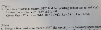 (25pts) 3. For a four resistors n-channel JFET, find the operating points (VGS, ID, and VDs). Assume Ipss = 5mA, Vp= -4.5V and IG-0 Given: Vpp = 12 V, Ri=2M.2, R2= 1.5M2, RD=6 k2, Rss = 4k12, (25pts) 4. Design a four resistors n-Channel JFET bias circuit for the following specificatio YTT -
7. Consider an ideal n-channel silicon MOSFET with the following device parameters: VT --0.8 V, μ...
 Vgs for part b, not Vds
7. Consider an ideal n-channel silicon MOSFET with the following device parameters: VT --0.8 V, μ,-425 cm2V-1 s-1, tox-11 nm, w: 20 μm' and L-1.2 μm at T-300 K. nm, W- 20 a) Plot the drain current ID [mA] versus drain-source voltage Vos over the range 0 < VD 3V with VGS--0.8 V, VGs 0 V and Vas +0.8 V b) Plot root saturation current ID12(sat) [mA12] versus gate-source voltage V6s over the range...
Vgs for part b, not Vds
7. Consider an ideal n-channel silicon MOSFET with the following device parameters: VT --0.8 V, μ,-425 cm2V-1 s-1, tox-11 nm, w: 20 μm' and L-1.2 μm at T-300 K. nm, W- 20 a) Plot the drain current ID [mA] versus drain-source voltage Vos over the range 0 < VD 3V with VGS--0.8 V, VGs 0 V and Vas +0.8 V b) Plot root saturation current ID12(sat) [mA12] versus gate-source voltage V6s over the range...
 The transfer characteristic curve plotted below is representing a n-channel E-MOSFET. Vos VGS(th) O True False Which among the following transistors is the most suited for high-speed and high-frequency applications? a. MOSFET b. BJT C. IGBT d. JFET For a device, the characteristic of the I-V curve is exhibited as below. - -VGS - a. BJT b. E-MOSFET c. D-MOSFET d. JFET In a JFET or MOSFET, the parameter of loss is denoting - a. drain to source current with...
 The ID–VDS of a 1980s vintage (but “ideal”) N-MOSFET is shown in
the figure. The VT = 1 V, tox = 100 nm
(SiO2) and the source is grounded. (a) What regions of operation do
points (1), (2), and (3) correspond to? (b) What is the applied
gate voltage? (c) What is the inversion charge density (in
electrons per cm2) at the source end of the channel, n(y = 0), and
at the drain end of the channel, n(y =...
The ID–VDS of a 1980s vintage (but “ideal”) N-MOSFET is shown in
the figure. The VT = 1 V, tox = 100 nm
(SiO2) and the source is grounded. (a) What regions of operation do
points (1), (2), and (3) correspond to? (b) What is the applied
gate voltage? (c) What is the inversion charge density (in
electrons per cm2) at the source end of the channel, n(y = 0), and
at the drain end of the channel, n(y =...
 3. A circuit for an n-channel depletion MOSFET is shown in below. The transistor parameters are V 25 V and lpss - 10 mA. Calculate the quiescent values of ID, Vps, and VGS Assume R 1 MO, R2 = 60 k 2 and Rolk. -- + 18V < R, ΟΜΩ SND 3 R 3600k
 Question 17 (1 point) The transconductance of an n-channel MOSFET is found to be Sm- lo/aVGs 1.75 mA/V when measured at VDs 50 mV. The threshold voltage is VT 0.5 V. What is the current at VGS-0.8 V and VDs 1.5 V? Use the conductance parameter Kn found previously. a) D 6.30 mA b) ID 7.21 mA c) D, 0.963 mA d) ID-0.695 mA
Question 17 (1 point) The transconductance of an n-channel MOSFET is found to be Sm- lo/aVGs...
Question 17 (1 point) The transconductance of an n-channel MOSFET is found to be Sm- lo/aVGs 1.75 mA/V when measured at VDs 50 mV. The threshold voltage is VT 0.5 V. What is the current at VGS-0.8 V and VDs 1.5 V? Use the conductance parameter Kn found previously. a) D 6.30 mA b) ID 7.21 mA c) D, 0.963 mA d) ID-0.695 mA
Question 17 (1 point) The transconductance of an n-channel MOSFET is found to be Sm- lo/aVGs...
 For the n-channel E-MOSFET transistor in the circuit, the
parameters are VT N = 0.4 V, Kn =
120μA/V2. Determine VGS, ID, and
VDS. Sketch the DC and AC load lines and plot the
Q-point. Assume AC input is connected to the gate and output is
connected to the drain.
+5 V S RD= 1.2 kΩ = 14 kΩ S R) = 6 ΚΩ: Rs= 0.5 ΚΩ –5 V
For the n-channel E-MOSFET transistor in the circuit, the
parameters are VT N = 0.4 V, Kn =
120μA/V2. Determine VGS, ID, and
VDS. Sketch the DC and AC load lines and plot the
Q-point. Assume AC input is connected to the gate and output is
connected to the drain.
+5 V S RD= 1.2 kΩ = 14 kΩ S R) = 6 ΚΩ: Rs= 0.5 ΚΩ –5 V
 (25pts) 3. For a four resistors n-channel JFET, find the operating points (VGS, ID, and VDs). Assume Ipss = 5mA, Vp= -4.5V and IG-0 Given: Vpp = 12 V, Ri=2M.2, R2= 1.5M2, RD=6 k2, Rss = 4k12, (25pts) 4. Design a four resistors n-Channel JFET bias circuit for the following specificatio YTT -
 Vgs for part b, not Vds
7. Consider an ideal n-channel silicon MOSFET with the following device parameters: VT --0.8 V, μ,-425 cm2V-1 s-1, tox-11 nm, w: 20 μm' and L-1.2 μm at T-300 K. nm, W- 20 a) Plot the drain current ID [mA] versus drain-source voltage Vos over the range 0 < VD 3V with VGS--0.8 V, VGs 0 V and Vas +0.8 V b) Plot root saturation current ID12(sat) [mA12] versus gate-source voltage V6s over the range...
Vgs for part b, not Vds
7. Consider an ideal n-channel silicon MOSFET with the following device parameters: VT --0.8 V, μ,-425 cm2V-1 s-1, tox-11 nm, w: 20 μm' and L-1.2 μm at T-300 K. nm, W- 20 a) Plot the drain current ID [mA] versus drain-source voltage Vos over the range 0 < VD 3V with VGS--0.8 V, VGs 0 V and Vas +0.8 V b) Plot root saturation current ID12(sat) [mA12] versus gate-source voltage V6s over the range...
Most questions answered within 3 hours.
-
Where is the error in this code sequence?
String s1 = "Hello";
String s2 = "ello";...
asked 11 months ago -
Financial data for Joel de Paris, Inc., for last year
follow:
Joel de Paris, Inc.
Balance...
asked 11 months ago -
Consider this reaction:
Al2(SO4)3 (aq)+ BaCl3
(aq) Al2Cl6 (aq)- +
3BaSO4(s) . What is the...
asked 11 months ago -
Suppose that Savneet is considering increasing her
recent random sample from 20 car rentals to 40...
asked 11 months ago -
Trucks arrive at an unloading terminal at an average rate of 120
per hour.
Trucks arrive...
asked 11 months ago -
Why are methanol and ethanol completely soluble in water while
octanol is not very little soluble....
asked 11 months ago -
A facilities manager at a university reads in a research report
that the mean amount of...
asked 11 months ago -
When the CuSO4 is rehydrated by adding water to the anhydrous
compound, is this an endothermic...
asked 11 months ago -
A ray of sunlight is passing from diamond into crown glass; the
angle of incidence is...
asked 11 months ago -
A block of mass 0.249 kg is placed on top of a light, vertical
spring of...
asked 11 months ago -
how do the kidneys compensate in the presences of acidosis
a) trigger hyperventilate
b) reserve acid...
asked 11 months ago -
Question 501 pts
The rental rate of capital to the firm increases. Which of the
following...
asked 11 months ago