With four Boolean inputs mentioned in the first four columns of the following table, report the...
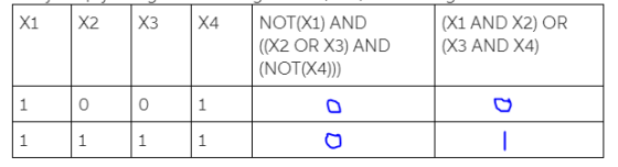
With four Boolean inputs mentioned in the first four columns of the following table, report the outputs from the circuits described by the Boolean expressions in the topmost row of the table in the 5th and 6th columns, in the corresponding rows in the 5th and 6th columns of the table. The circuit in the 5th column uses two AND gates, two NOT gates, and one OR gate. The circuit in the 6th column uses two AND gates and one OR gate. You can draw the circuits or construct partial truth tables which have just the given combinations of input values instead of the 16 possible combinations, if you wish. You can also find the answers by simply using the meaning of AND, OR, and NOT gates.
|
X1 |
X2 |
X3 |
X4 |
NOT(X1) AND ((X2 OR X3) AND (NOT(X4))) |
(X1 AND X2) OR (X3 AND X4) |
|
1 |
0 |
0 |
1 |
||
|
1 |
1 |
1 |
1 |
Homework Answers
// If you want anything else please comment
// i give only output basis of OR and AND
Add Answer to:
With four Boolean inputs mentioned in the first four columns of
the following table, report the...
Consider the following four types of gates: AND, OR, NAND and NOR. If we assign one...
Consider the following four types of gates: AND, OR, NAND and NOR. If we assign one type of gate for the first level and one type for the second level, we find that there are 16 possible combinations of two-level forms. Eight of these combinations are said to be degenerate forms because they result in a single Boolean operation. List these eight degenerate combinations and show why this is the case, resulting in extending the number of inputs to a...
Design a circuit to add two 2-bit binary numbers and display the results of the addition...
Design a circuit to add two 2-bit binary numbers and display the results of the addition as a 3-bit binary number, with the most significant bit be the carry out. To do this, you will use the four switches on your Breadboard Companion as your two 2-bit number inputs. Three of your LEDs will be used to represent the 3-bit output of your circuit. Complete a truth table for the expected output values on the lab data sheet attached. Use...
8. For this problem, you are to design a simple combinational logic circuit and then use...
 8. For this problem, you are to design a simple combinational logic circuit and then use Logisim to simulate and test the circuit. The circuit is a 2- bit priority encoder with inputs X2 and X1 and outputs Y1 and Yo. The circuit behaves as follows: oIf X2X1 00, then Y1Yo 00 (no active input) If X2X1 01, then Y1Yo = 01 (low-priority input, X1, is active) If X2X1 1-, then Y1Y0 10 (high-priority input, X2, is active) Note that...
This was the answer I got, teacher said it was wrong Teacher said, couldnt run the...
 This was the answer I got, teacher said it was wrong
Teacher said, couldnt run the gate because there wasnt any
switches
5. Design and test a simplified logic circuit to identify all numbers in the output range of function: F(x) = 2x+3 for an input domain between 0 and 6. Be sure to include your truth table. Normal 1 No Spac... Heading 1 Head Paragraph Styles t Draw Simulate View Window Help 39 ) ) 11:55 1 esu.desire2learn.com Boolean...
This was the answer I got, teacher said it was wrong
Teacher said, couldnt run the gate because there wasnt any
switches
5. Design and test a simplified logic circuit to identify all numbers in the output range of function: F(x) = 2x+3 for an input domain between 0 and 6. Be sure to include your truth table. Normal 1 No Spac... Heading 1 Head Paragraph Styles t Draw Simulate View Window Help 39 ) ) 11:55 1 esu.desire2learn.com Boolean...
Building and testing basic combinational circuits using Verilog HDL Description: Build and test the following circuits using gate-level modeling in Verilog HDL 1.3-input majority function 2.Condition...
 Building and testing basic combinational circuits using Verilog HDL Description: Build and test the following circuits using gate-level modeling in Verilog HDL 1.3-input majority function 2.Conditional inverter (see the table below: x - control input, y -data input). Do NOT use XOR gates for the implementation. Output 3. Two-input multiplexer (see the table below: x.y -data inputs, z- control input) Output 4. 1-bit half adder. 5. 1-bit full adder by cascading two half adders 6.1-bit full adder directly (as in...
Tim Question 1 Atte 20 pts 2H 24 Design a 1-bit Full Adder using NOR gates...
 Tim Question 1 Atte 20 pts 2H 24 Design a 1-bit Full Adder using NOR gates only, you must include and show: Truth tables, detail logic gate circuit designs, and Boolean expressions Upload Choose a File 20 pts Question 2 Design a 4-bit Full Adder with inputs (Xo...X3, Yo...Y3) in which inputs X are connect to two 4-bit registers via four 2-to-1 Multiplexers and inputs Y are connected to two other 4-bit registers via four 2-to-1 Multiplexers. In this case...
A comparator circuit has two 1-bit inputs A and B and three 1-bit outputs G (greater),...
A comparator circuit has two 1-bit inputs A and B and three 1-bit outputs G (greater), E (equal), and L (less than). That is, G is 1 if A > B (0 otherwise), E is 1 if A == B (0 otherwise), and L is 1 if A < B (0 otherwise). a. Draw the truth table for a 1-bit comparator (the table has 2 inputs and 3 outputs). b. Implement G, E, and L circuits using only...
Building and testing basic combinational circuits using Verilog HDL Description: Build and test t...
Building and testing basic combinational circuits using Verilog HDL Description: Build and test the following circuits using gate-level modeling in Verilog HDL. 1. 3-input majority function. 2. Conditional inverter (see the table below: x - control input, y - data input). Do NOT use XOR gates for the implementation. x y Output 0 y 1 y' 3. Two-input multiplexer (see the table below: x,y - data inputs, z - control input). z Output 0 x 1 y 4. 1-bit half...
Multiplexer Example Implement the following Boolean function using a 4x1 Mux;
 Multiplexer Example Implement the following Boolean function using a 4x1 Mux; F(x,y,z) = Σ (1,2,6,7) Decoder Example Implement the following functions for a full adder using decoder; S(x,y,z) = Σ (1,2,4,7) C(x,y,z) = Σ (3,5,6,7) Implement the following Boolean function; F(x,y,z) = Σ (0,2,3,7): Using; 1. Two 2x4 decoders and logic gates 2. One 4x1 multiplexer Decoder . Draw the truth table for the function to be implemented. . Pick the terms for output. . Derive appropriate logic to combine terms. . Use two 2x4 decoders to make one3x8 decoder. . Pay attention to fact...
Part 1 This section is just a quick check to make sure you understand how the...
 Part 1 This section is just a quick check to make sure you understand how the equipment works. The circuit does not provide any useful function Nodes A and B represent inputs from the switch board while X represents an output displayed on an LED Check the chip information provided for chip pin-outs in particular the power supply connections. In general, you should place a couple of 100nF Multi-layer-ceramic (MLC) capacitors across the power supply lines to reduce electrical noise....
 8. For this problem, you are to design a simple combinational logic circuit and then use Logisim to simulate and test the circuit. The circuit is a 2- bit priority encoder with inputs X2 and X1 and outputs Y1 and Yo. The circuit behaves as follows: oIf X2X1 00, then Y1Yo 00 (no active input) If X2X1 01, then Y1Yo = 01 (low-priority input, X1, is active) If X2X1 1-, then Y1Y0 10 (high-priority input, X2, is active) Note that...
 This was the answer I got, teacher said it was wrong
Teacher said, couldnt run the gate because there wasnt any
switches
5. Design and test a simplified logic circuit to identify all numbers in the output range of function: F(x) = 2x+3 for an input domain between 0 and 6. Be sure to include your truth table. Normal 1 No Spac... Heading 1 Head Paragraph Styles t Draw Simulate View Window Help 39 ) ) 11:55 1 esu.desire2learn.com Boolean...
This was the answer I got, teacher said it was wrong
Teacher said, couldnt run the gate because there wasnt any
switches
5. Design and test a simplified logic circuit to identify all numbers in the output range of function: F(x) = 2x+3 for an input domain between 0 and 6. Be sure to include your truth table. Normal 1 No Spac... Heading 1 Head Paragraph Styles t Draw Simulate View Window Help 39 ) ) 11:55 1 esu.desire2learn.com Boolean...
 Building and testing basic combinational circuits using Verilog HDL Description: Build and test the following circuits using gate-level modeling in Verilog HDL 1.3-input majority function 2.Conditional inverter (see the table below: x - control input, y -data input). Do NOT use XOR gates for the implementation. Output 3. Two-input multiplexer (see the table below: x.y -data inputs, z- control input) Output 4. 1-bit half adder. 5. 1-bit full adder by cascading two half adders 6.1-bit full adder directly (as in...
 Tim Question 1 Atte 20 pts 2H 24 Design a 1-bit Full Adder using NOR gates only, you must include and show: Truth tables, detail logic gate circuit designs, and Boolean expressions Upload Choose a File 20 pts Question 2 Design a 4-bit Full Adder with inputs (Xo...X3, Yo...Y3) in which inputs X are connect to two 4-bit registers via four 2-to-1 Multiplexers and inputs Y are connected to two other 4-bit registers via four 2-to-1 Multiplexers. In this case...
 Part 1 This section is just a quick check to make sure you understand how the equipment works. The circuit does not provide any useful function Nodes A and B represent inputs from the switch board while X represents an output displayed on an LED Check the chip information provided for chip pin-outs in particular the power supply connections. In general, you should place a couple of 100nF Multi-layer-ceramic (MLC) capacitors across the power supply lines to reduce electrical noise....
Most questions answered within 3 hours.
-
Where is the error in this code sequence?
String s1 = "Hello";
String s2 = "ello";...
asked 11 months ago -
Financial data for Joel de Paris, Inc., for last year
follow:
Joel de Paris, Inc.
Balance...
asked 11 months ago -
Consider this reaction:
Al2(SO4)3 (aq)+ BaCl3
(aq) Al2Cl6 (aq)- +
3BaSO4(s) . What is the...
asked 11 months ago -
Suppose that Savneet is considering increasing her
recent random sample from 20 car rentals to 40...
asked 11 months ago -
Trucks arrive at an unloading terminal at an average rate of 120
per hour.
Trucks arrive...
asked 11 months ago -
Why are methanol and ethanol completely soluble in water while
octanol is not very little soluble....
asked 11 months ago -
A facilities manager at a university reads in a research report
that the mean amount of...
asked 11 months ago -
When the CuSO4 is rehydrated by adding water to the anhydrous
compound, is this an endothermic...
asked 11 months ago -
A ray of sunlight is passing from diamond into crown glass; the
angle of incidence is...
asked 11 months ago -
A block of mass 0.249 kg is placed on top of a light, vertical
spring of...
asked 11 months ago -
how do the kidneys compensate in the presences of acidosis
a) trigger hyperventilate
b) reserve acid...
asked 11 months ago -
Question 501 pts
The rental rate of capital to the firm increases. Which of the
following...
asked 11 months ago