code in Verilog please. modify the code below to make a PCAdder to implement an adder...
code in Verilog please.
modify the code below to make a PCAdder to implement an adder that always adds one input by 4. And make testbench for testing of 2 cases. Thank you!
*CODE BELOW*
module PCAdder(PCResult, PCAddResult);
input [31:0] PCResult;
output reg [31:0] PCAddResult;
/* Please fill in the implementation here... */
endmodule
Homework Answers
Verilog Module : PCAdder.v
`timescale 1ns / 1ps
module PCAdder(
input [31:0] PCResult,
output [31:0] PCAddResult
);
assign PCAddResult=PCResult+4;
endmodule
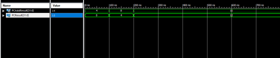
Verilog Test bench :PCAdder_tb.v
`timescale 1ns / 1ps
module PCAdder_tb;
// Inputs
reg [31:0] PCResult;
// Outputs
wire [31:0] PCAddResult;
// Instantiate the Unit Under Test (UUT)
PCAdder uut (
.PCResult(PCResult),
.PCAddResult(PCAddResult)
);
initial begin
// Initialize Inputs
PCResult = 0;
// Wait 100 ns for global reset
to finish
// Add stimulus here
#100;
PCResult=4; //Test case 1
#100; //wait for 100 ns
PCResult=12; //Test case 2
end
endmodule
Add Answer to:
code in Verilog please.
modify the code below to make a PCAdder to implement an adder...
3. (10 Points) RTL Combinational Circuit Design a Draw the schematic for the Verilog code given...
 3. (10 Points) RTL Combinational Circuit Design a Draw the schematic for the Verilog code given below: module abc (a, b, c, d, si, s0); input 31, 30; output a, b, c,d; not (51_, 51), (50_, 0); and (a, s1_, SO_); and (b, s1_, 0); and (c, sl, s0_); and (d, sl, s0); endmodule b. Draw the schematic for the Verilog code given below: module Always_Code input a, b, c, output reg F ); always @(a, b, c) begin F...
Please help to complete the code and write the testbench to design the following adder. 1.In...
Please help to complete the code and write the testbench to design the following adder. 1.In this section, you add pipeline stage. 8 bits are used at every pipeline stage.Use the following template to complete your Verilog coding. // Addition of two 16 bit, 2's complement nos., n1 and n2. 8 bits addition at a time. Result is 17 bits. module adder_b (clk, n1, n2, sum) ; input clk ; input [15:0] n1 ; input [15:0] n2 ; output [16:0]...
a Read the following codes in Verilog and the corresponding testbench file. Describe what the codes...
a Read the following codes in Verilog and the corresponding testbench file. Describe what the codes are doing by adding comments in the code. Then write down the simulation results of res1, res2, res3, and res4, respectively. Source code module vector_defn (num1, res1, res2, res3, res4); input [7:0] num1; output res1; output [3:0] res2; output [0:7] res3; output [15:0] res4; assign res1=num1[2]; assign res2=num1[7:4]; assign res3=num1; assign res4={2{num1}}; endmodule testbench: `timescale 1ns / 1ps module vector_defn_tb; reg [7:0] in1; wire...
Note: not just code for an adder! Verilog code for a 32 bit MIPS Processor unit....
 Note: not just code for an adder!
Verilog code for a 32 bit MIPS Processor unit. (NOT pipelined). Please include all code, a testbench code and the software used. (Please do not give code already online). Thank vou!
Note: not just code for an adder!
Verilog code for a 32 bit MIPS Processor unit. (NOT pipelined). Please include all code, a testbench code and the software used. (Please do not give code already online). Thank vou!
Please explain what he verilog code does: module lab7_2_3( input clk, input Enable, input Clear, input...
Please explain what he verilog code does: module lab7_2_3( input clk, input Enable, input Clear, input Load, output [3:0] Q, reg [3:0] count, wire cnt_done ); assign cnt_done = ~| count; assign Q = count; always @(posedge clk) if (Clear) count <= 0; else if (Enable) if (Load | cnt_done) count <= 4'b1010; // decimal 10 else count <= count - 1; Endmodule
Please code the following in Verilog: Write the HDL gate-level hierarchical description of a four-bit adder-subtractor...
 Please code the following in Verilog:
Write the HDL gate-level hierarchical description of a four-bit adder-subtractor for unsigned binary numbers similar to the following circuit. You can instantiate the four-bit full adder described in the following example code Figure 4.13a, 4-Bit adder-subtractor without overflow Inputs: 4-Bit A, 4-Bit B, and Mode M (0-add/1-subtract) Interfaces: Carry Bits C1, C2, C3 Outputs: Carry C (1 Bit, C4), Sum S (4 bit) Bo A FA FA FA FA module Add half (input a,...
Please code the following in Verilog:
Write the HDL gate-level hierarchical description of a four-bit adder-subtractor for unsigned binary numbers similar to the following circuit. You can instantiate the four-bit full adder described in the following example code Figure 4.13a, 4-Bit adder-subtractor without overflow Inputs: 4-Bit A, 4-Bit B, and Mode M (0-add/1-subtract) Interfaces: Carry Bits C1, C2, C3 Outputs: Carry C (1 Bit, C4), Sum S (4 bit) Bo A FA FA FA FA module Add half (input a,...
Write the verilog code that implements a negitive edge D-Flip Flop with asynchronous active low preset...
Write the verilog code that implements a negitive edge D-Flip Flop with asynchronous active low preset and clear I have : module dff( preset, clear, clk, D, Q) input preset; input clear; input clk; input D; output Q; reg Q; always @ (negedge clk or negedge preset or negedge clear); if (preset); Q = 0; else (clear == 0); Q = D; endmodule I honestly just want to know if i'm doing this right or not, if im not correct,...
Write a testbench for use in Quartus' ModelSim Altera in verilog for the following code of...
Write a testbench for use in Quartus' ModelSim Altera in verilog for the following code of a 4x16 register: module regFile4x16 (input clk, input write, input [2:0] wrAddr, input [15:0] wrData, input [2:0] rdAddrA, output [15:0] rdDataA, input [2:0] rdAddrB, output [15:0] rdDataB); reg [15:0] reg0, reg1, reg2, reg3; assign rdDataA = rdAddrA == 0 ? reg0 : rdAddrA == 1 ? reg1 : rdAddrA == 2 ? reg2 : rdAddrA == 3...
Write a test bench to thoroughly test the Verilog module dff_fe_asyn_h. below is the module ddff_fe_asyn_h.code...
Write a test bench to thoroughly test the Verilog module dff_fe_asyn_h. below is the module ddff_fe_asyn_h.code Simulate the circuit using ISim and analyze the resulting waveform. Verilog Code for dff_fe_asyn_h is mentioned below:- //DFF module with asynchronous active high reset with negative edge trigger with clock module dff_fe_asyn_h ( input clock, // Clock Input input reset, // Reset Input input data_in, // Input Data output reg data_out // Output Data ); always @ (negedge clock or posedge reset) // triggers...
Question 3: Realize the circuit below using Verilog. Include a signal “reset_n” for asynchronously clearing the...
 Question 3: Realize the circuit below using Verilog. Include a signal “reset_n” for asynchronously clearing the flip-flop. What type of circuit is this? Complete the following Verilog code. Write a test bench to test it. clk sel module aff (clk, reset_n, sel, q); input clk ; // Declare the inputs and outputs of the module. input reset_n; input sel; output q; reg q; wire D; ; // model the combinational logic assign D= always @( begin if ( else end...
 3. (10 Points) RTL Combinational Circuit Design a Draw the schematic for the Verilog code given below: module abc (a, b, c, d, si, s0); input 31, 30; output a, b, c,d; not (51_, 51), (50_, 0); and (a, s1_, SO_); and (b, s1_, 0); and (c, sl, s0_); and (d, sl, s0); endmodule b. Draw the schematic for the Verilog code given below: module Always_Code input a, b, c, output reg F ); always @(a, b, c) begin F...
 Note: not just code for an adder!
Verilog code for a 32 bit MIPS Processor unit. (NOT pipelined). Please include all code, a testbench code and the software used. (Please do not give code already online). Thank vou!
Note: not just code for an adder!
Verilog code for a 32 bit MIPS Processor unit. (NOT pipelined). Please include all code, a testbench code and the software used. (Please do not give code already online). Thank vou!
 Please code the following in Verilog:
Write the HDL gate-level hierarchical description of a four-bit adder-subtractor for unsigned binary numbers similar to the following circuit. You can instantiate the four-bit full adder described in the following example code Figure 4.13a, 4-Bit adder-subtractor without overflow Inputs: 4-Bit A, 4-Bit B, and Mode M (0-add/1-subtract) Interfaces: Carry Bits C1, C2, C3 Outputs: Carry C (1 Bit, C4), Sum S (4 bit) Bo A FA FA FA FA module Add half (input a,...
Please code the following in Verilog:
Write the HDL gate-level hierarchical description of a four-bit adder-subtractor for unsigned binary numbers similar to the following circuit. You can instantiate the four-bit full adder described in the following example code Figure 4.13a, 4-Bit adder-subtractor without overflow Inputs: 4-Bit A, 4-Bit B, and Mode M (0-add/1-subtract) Interfaces: Carry Bits C1, C2, C3 Outputs: Carry C (1 Bit, C4), Sum S (4 bit) Bo A FA FA FA FA module Add half (input a,...
 Question 3: Realize the circuit below using Verilog. Include a signal “reset_n” for asynchronously clearing the flip-flop. What type of circuit is this? Complete the following Verilog code. Write a test bench to test it. clk sel module aff (clk, reset_n, sel, q); input clk ; // Declare the inputs and outputs of the module. input reset_n; input sel; output q; reg q; wire D; ; // model the combinational logic assign D= always @( begin if ( else end...
Most questions answered within 3 hours.
-
Where is the error in this code sequence?
String s1 = "Hello";
String s2 = "ello";...
asked 11 months ago -
Financial data for Joel de Paris, Inc., for last year
follow:
Joel de Paris, Inc.
Balance...
asked 11 months ago -
Consider this reaction:
Al2(SO4)3 (aq)+ BaCl3
(aq) Al2Cl6 (aq)- +
3BaSO4(s) . What is the...
asked 11 months ago -
Suppose that Savneet is considering increasing her
recent random sample from 20 car rentals to 40...
asked 11 months ago -
Trucks arrive at an unloading terminal at an average rate of 120
per hour.
Trucks arrive...
asked 11 months ago -
Why are methanol and ethanol completely soluble in water while
octanol is not very little soluble....
asked 11 months ago -
A facilities manager at a university reads in a research report
that the mean amount of...
asked 11 months ago -
When the CuSO4 is rehydrated by adding water to the anhydrous
compound, is this an endothermic...
asked 11 months ago -
A ray of sunlight is passing from diamond into crown glass; the
angle of incidence is...
asked 11 months ago -
A block of mass 0.249 kg is placed on top of a light, vertical
spring of...
asked 11 months ago -
how do the kidneys compensate in the presences of acidosis
a) trigger hyperventilate
b) reserve acid...
asked 11 months ago -
Question 501 pts
The rental rate of capital to the firm increases. Which of the
following...
asked 11 months ago