Use the gated SR latch design with only NAND gates to design a gated SR flip–flop....
Use the gated SR latch design with only NAND gates to design a gated SR flip–flop. The stored bit Q can only change on the positive edge (rising edge) of the clock cycle. Draw the circuit using only logic gates and create a symbol for the flip–flop you designed.
Homework Answers
Given problem has been solved with proper design and explanation. To understand this problem, a basic knowledge of SR Flip flop is required. If you have any doubt, please comment.
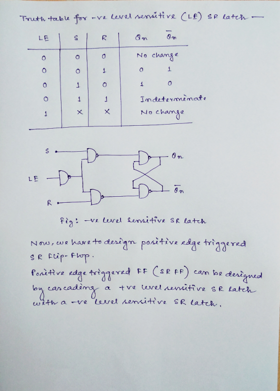
Here, level sensitive SR latches are gated SR latches.


Add Answer to:
Use the gated SR latch design with only NAND gates to design a
gated SR flip–flop....
-Design a gated SR latch using NAND or NOR gates. -Design a negative edge D master-slave...
-Design a gated SR latch using NAND or NOR gates. -Design a negative edge D master-slave flip-flop using the SR latch designed above -Design the D-flip-flop using the “truly” edge-triggered approach using NOR gates
a) (5 marks) Explain the difference between a latch, a gated latch and a flip flop....
 a) (5 marks) Explain the difference between a latch, a gated latch and a flip flop. b) (5 marks) A gated SR latch has the following schematic diagram CLK a) Draw a timing diagram showing the Q and Q outputs for the following sequence of inputs: CLK R Assume that the initial state of the outputs is Q 0 and Q 1 c) (5 marks) Draw a schematic diagram for a rising edge-triggered master-slave D flip- flop built using two...
5.4 2um 4-34. Design a negative-edge-triggered flip-flop. The flip flop has three inputs; these are Data,...
 5.4 2um
4-34. Design a negative-edge-triggered flip-flop. The flip flop has three inputs; these are Data, Clock, and Enable. If, at the negative edge of the clock, the enable input equals to 0, then the state at Data input is stored in the flip-flop. If, at the negative edge of clock, Enable is in 1 state, then the current stored value in the flip-flop is held. Design the flip-flop using only SR latches, AND gates, and NOT gates.
4-34. Design...
5.4 2um
4-34. Design a negative-edge-triggered flip-flop. The flip flop has three inputs; these are Data, Clock, and Enable. If, at the negative edge of the clock, the enable input equals to 0, then the state at Data input is stored in the flip-flop. If, at the negative edge of clock, Enable is in 1 state, then the current stored value in the flip-flop is held. Design the flip-flop using only SR latches, AND gates, and NOT gates.
4-34. Design...
a) Draw an SR-latch using only NAND gates. Label each input and output, and label all...
a) Draw an SR-latch using only NAND gates. Label each input and output, and label all wires with a name if the wire does not connect to any input or output b) Describe the behavior of the latch when S and R are both 0. What is the output of each gate? c) Assuming that the latch starts with S = R = 0, write down the sequence of what happens when R = 1. Discuss changes at each point...
a) Draw SR latch impeltation in NOR gates provied function table b) Show how D latch...
a) Draw SR latch impeltation in NOR gates provied function table b) Show how D latch (transprent) can be made from NOR gate. SR latch is transprent when it comes to storing data. c) What is limitation of D latch in terms of storing data ? what does it achive for digital terms d) Design a D flip flop that is -ve edge trigged using master slave combination of D latches designed in b) Inverters may be needed.
Design a positive-edge T flip-flop using a positive-edge-triggered D flip-flop and other logic gates.
Design a positive-edge T flip-flop using a positive-edge-triggered D flip-flop and other logic gates.
Use the Quartus Prime Text Editor to implement a behavioral model of the D flip-flop described ab...
 Use the Quartus Prime Text Editor to implement a behavioral
model of the D flip-flop described above in a file named
d_flops.sv. Specify the D flip-flop’s module according to the
interface specification given in the table below.
Port
Mode
Data Type
Size
Description
RST
in
logic
1-bit
Active high asynchronous reset
CLK
in
logic
1-bit
Synchronizing clock signal
EN
in
logic
1-bit
Synchronous clock enable
D
in
logic
1-bit
Synchronous data input
Q
out
logic
1-bit
Current/present state
Qbar
out...
Use the Quartus Prime Text Editor to implement a behavioral
model of the D flip-flop described above in a file named
d_flops.sv. Specify the D flip-flop’s module according to the
interface specification given in the table below.
Port
Mode
Data Type
Size
Description
RST
in
logic
1-bit
Active high asynchronous reset
CLK
in
logic
1-bit
Synchronizing clock signal
EN
in
logic
1-bit
Synchronous clock enable
D
in
logic
1-bit
Synchronous data input
Q
out
logic
1-bit
Current/present state
Qbar
out...
Draw the gate level circuit schematic of a D flip-flop and a T flip-flop based on the cross-coupled NAND latch. Briefly discuss the timing behavior of a D flip-flop, a T flip-flop and a latch. (a) (8...
 Draw the gate level circuit schematic of a D flip-flop and a T flip-flop based on the cross-coupled NAND latch. Briefly discuss the timing behavior of a D flip-flop, a T flip-flop and a latch. (a) (8 Marks) circuit has three inputs, S, C and C2. S is the control input. When S-O, the circuit behaves like a D flip-flop, and when S-1, the circuit behaves like a T flip-flop. The input characteristics of the circuit are tabulated in Table...
1- A) The SR latch is different from combinational circuits because it preserves state. That is,...
1- A) The SR latch is different from combinational circuits because it preserves state. That is, unlike combinational circuits, if the inputs change, the circuit keeps its present state. Say that the present state of the SR latch is “set”. We change the values on the two input pins, and the state does not change. What is the value on those input pins? 1- B) Assume that you have a D flip-flop module available to you. Treat it like a...
Provide a complementary CMOS transistor circuit design for a a) NOR based SR flip-flop b) NAND...
 Provide a complementary CMOS transistor circuit design for a a) NOR based SR flip-flop b) NAND based SR flip-flop
 a) (5 marks) Explain the difference between a latch, a gated latch and a flip flop. b) (5 marks) A gated SR latch has the following schematic diagram CLK a) Draw a timing diagram showing the Q and Q outputs for the following sequence of inputs: CLK R Assume that the initial state of the outputs is Q 0 and Q 1 c) (5 marks) Draw a schematic diagram for a rising edge-triggered master-slave D flip- flop built using two...
 5.4 2um
4-34. Design a negative-edge-triggered flip-flop. The flip flop has three inputs; these are Data, Clock, and Enable. If, at the negative edge of the clock, the enable input equals to 0, then the state at Data input is stored in the flip-flop. If, at the negative edge of clock, Enable is in 1 state, then the current stored value in the flip-flop is held. Design the flip-flop using only SR latches, AND gates, and NOT gates.
4-34. Design...
5.4 2um
4-34. Design a negative-edge-triggered flip-flop. The flip flop has three inputs; these are Data, Clock, and Enable. If, at the negative edge of the clock, the enable input equals to 0, then the state at Data input is stored in the flip-flop. If, at the negative edge of clock, Enable is in 1 state, then the current stored value in the flip-flop is held. Design the flip-flop using only SR latches, AND gates, and NOT gates.
4-34. Design...
 Use the Quartus Prime Text Editor to implement a behavioral
model of the D flip-flop described above in a file named
d_flops.sv. Specify the D flip-flop’s module according to the
interface specification given in the table below.
Port
Mode
Data Type
Size
Description
RST
in
logic
1-bit
Active high asynchronous reset
CLK
in
logic
1-bit
Synchronizing clock signal
EN
in
logic
1-bit
Synchronous clock enable
D
in
logic
1-bit
Synchronous data input
Q
out
logic
1-bit
Current/present state
Qbar
out...
Use the Quartus Prime Text Editor to implement a behavioral
model of the D flip-flop described above in a file named
d_flops.sv. Specify the D flip-flop’s module according to the
interface specification given in the table below.
Port
Mode
Data Type
Size
Description
RST
in
logic
1-bit
Active high asynchronous reset
CLK
in
logic
1-bit
Synchronizing clock signal
EN
in
logic
1-bit
Synchronous clock enable
D
in
logic
1-bit
Synchronous data input
Q
out
logic
1-bit
Current/present state
Qbar
out...
 Draw the gate level circuit schematic of a D flip-flop and a T flip-flop based on the cross-coupled NAND latch. Briefly discuss the timing behavior of a D flip-flop, a T flip-flop and a latch. (a) (8 Marks) circuit has three inputs, S, C and C2. S is the control input. When S-O, the circuit behaves like a D flip-flop, and when S-1, the circuit behaves like a T flip-flop. The input characteristics of the circuit are tabulated in Table...
 Provide a complementary CMOS transistor circuit design for a a) NOR based SR flip-flop b) NAND based SR flip-flop
Most questions answered within 3 hours.
-
Where is the error in this code sequence?
String s1 = "Hello";
String s2 = "ello";...
asked 11 months ago -
Financial data for Joel de Paris, Inc., for last year
follow:
Joel de Paris, Inc.
Balance...
asked 11 months ago -
Consider this reaction:
Al2(SO4)3 (aq)+ BaCl3
(aq) Al2Cl6 (aq)- +
3BaSO4(s) . What is the...
asked 11 months ago -
Suppose that Savneet is considering increasing her
recent random sample from 20 car rentals to 40...
asked 11 months ago -
Trucks arrive at an unloading terminal at an average rate of 120
per hour.
Trucks arrive...
asked 11 months ago -
Why are methanol and ethanol completely soluble in water while
octanol is not very little soluble....
asked 11 months ago -
A facilities manager at a university reads in a research report
that the mean amount of...
asked 11 months ago -
When the CuSO4 is rehydrated by adding water to the anhydrous
compound, is this an endothermic...
asked 11 months ago -
A ray of sunlight is passing from diamond into crown glass; the
angle of incidence is...
asked 11 months ago -
A block of mass 0.249 kg is placed on top of a light, vertical
spring of...
asked 11 months ago -
how do the kidneys compensate in the presences of acidosis
a) trigger hyperventilate
b) reserve acid...
asked 11 months ago -
Question 501 pts
The rental rate of capital to the firm increases. Which of the
following...
asked 11 months ago