
Homework Answers
We shall solve this problem in a step-by-step manner
Before answering iv) we have to look at the results we get after solving i) and ii).
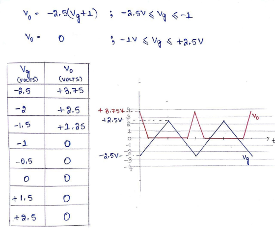
It gives two regions of operation
the region of operation 1) Diode D1 is off and Diode D2 is on when Vg is varying from -2.5V to -1V
the region of operation 2) Diode D1 is on and Diode D2 is off when Vg is varying from -1V to +2.5V
Draw the circuit during the first region of operation (ie Diode D1 is off and Diode D2 is on)

Now analyse the circuit and solve for Vo which will give the output voltage variation when Vg is between -2.5V to -1V
Use KCL and virtual short concept for analysis
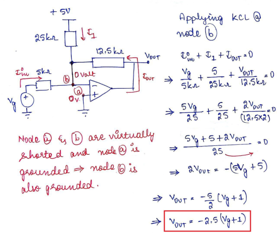
Draw the circuit during the second region of operation (ie Diode D1 is on and Diode D2 is off) and analyse the circuit
Here (since Diode D2 is off) Vo is freely hanging connected to node b through 12.5kohm. Also, node b is grounded because of virtual ground concept. Hence it is as good as Vo is grounded.

Now draw the input-output waveform
Add Answer to:
Just question iv)plz
n operational amplifier circuit is shown in Figure 3-1 +5 V 25 kQ...
a The operational amplifier in Figure 3.a has a slew rate of 0.5V/us and a unity gain bandwid of 5 MHz. Determine () the voltage gain, and (ii) the maximum input frequency such that the output wa...
 a The operational amplifier in Figure 3.a has a slew rate of 0.5V/us and a unity gain bandwid of 5 MHz. Determine () the voltage gain, and (ii) the maximum input frequency such that the output waveform is undistorted. with Vpeak 1V and frequency f. () Determine the cutoff frequency, (ii) plot, to scale, the you use this integrator if the input frequency is 30 KHz? Explain your answer. that any feedback resistance is fixed to 5k2. b. In the...
A common source amplifier circuit based on a single n-channel MOSFET is shown in Figure 4b. Assume that the transconductance gm-60 mS (equivalent to mA/ V) and drain source resistance, os,...
 A common source amplifier circuit based on a single n-channel MOSFET is shown in Figure 4b. Assume that the transconductance gm-60 mS (equivalent to mA/ V) and drain source resistance, os, is so large it may be neglected. 0) Calculate the open circuit voltage gain Av Yout/ Vis. i) The amplifier has a load of 10 k2. Determine the current gain Va. = 12 V 150k 4k3 Vout Vin 200k GND = 0 V Figure 4b a) State the name...
Laboratory 1: operation amplifier characteristics A. Objectives: 1. To study the basic characteri...
 thanks
Laboratory 1: operation amplifier characteristics A. Objectives: 1. To study the basic characteristics of an operational amplifier 2. To study the bias circuit of an operational amplifier B. Apparatus: 1. DC Power supply 2. Experimental board and corresponding components 3. Electronic calculator (prepared by students) 4. Digital camera (prepared by students for photo taking of the experimental results) 5. Laptop computer with the software PicoScope 6 and Microsoft Word installed. 6. PicoScope PC Oscilloscope and its accessories. 7. Multimeter...
thanks
Laboratory 1: operation amplifier characteristics A. Objectives: 1. To study the basic characteristics of an operational amplifier 2. To study the bias circuit of an operational amplifier B. Apparatus: 1. DC Power supply 2. Experimental board and corresponding components 3. Electronic calculator (prepared by students) 4. Digital camera (prepared by students for photo taking of the experimental results) 5. Laptop computer with the software PicoScope 6 and Microsoft Word installed. 6. PicoScope PC Oscilloscope and its accessories. 7. Multimeter...
IV, Laboratory Procedure 1. Construct the circuit of Figure 6.1, measure the current value 2. Con...
 IV, Laboratory Procedure 1. Construct the circuit of Figure 6.1, measure the current value 2. Construct the circuit of Figure 6.2; measure Vn and v., using the oscilloscope. 3. Construct the circuit of Figure 6.3, measure the value of Io and V 4. Construct the clipper design circuit, Capture the input and output waveforms. 5. Construct your clamper design circuit. Capture the input and output waveforms Figure 6.3 Design a clipper circuit which limits input signals to +3V and -2V....
An amplifier circuit using a bipolar transistor is shown in Figure Q5. (a) State, with a valid re...
 An amplifier circuit using a bipolar transistor is shown in
Figure Q5.
(a) State, with a valid reason, whether this amplifier is an
emitter follower
or a common emitter configuration.
(b) Redraw Figure Q5 as a large signal equivalent circuit. Show
that:
(c) Show that the input voltage, vISAT to produce the onset of
saturation for
T1 is given by:
(d), confirm, by calculation, that
T1 is in saturation.
(e) Calculate the current in the lamp when T1 is in...
An amplifier circuit using a bipolar transistor is shown in
Figure Q5.
(a) State, with a valid reason, whether this amplifier is an
emitter follower
or a common emitter configuration.
(b) Redraw Figure Q5 as a large signal equivalent circuit. Show
that:
(c) Show that the input voltage, vISAT to produce the onset of
saturation for
T1 is given by:
(d), confirm, by calculation, that
T1 is in saturation.
(e) Calculate the current in the lamp when T1 is in...
Question 2: Conditioning CIPeuIL A. The circuit in Figure 1 is used to amplify the input...
 Question 2: Conditioning CIPeuIL A. The circuit in Figure 1 is used to amplify the input signal sh output waveform, labelling both the x and y axis (both numb and explain in detail why the signal has the shape it hass and labels) necessary calculations to support your answer. it has, including any 23ks2 +10V 2.3kΩ sin(10t)V10V Figure 1 B. The circuit in Figure 2 is a full ECG amplifier circuit. Page 2 of6 47 nF UA 1 k2 33...
QUESTION 1 Figure Q1 shows a common emitter (CE) and common Base (CB) cascade amplifier circuit....
 QUESTION 1 Figure Q1 shows a common emitter (CE) and common Base (CB) cascade amplifier circuit. Determine the input and output impedance, Z; and Zo, voltage gain, Avi and Av2 and total cascade voltage gain, Ayr and Ays. [25 marks) 2 +8V 1.5 kn 2.2 F 82 k2 3.3 k2 Vo 2.2 uf B = 100 6.8 k12 1 k 2 what B = 100 tuf ZA 5.6 k 2 47012 ZA V. 33 k2 IuF w 10k_2 -2V w...
02 +Vo D3 Rgare 18 Circuit for Problem 1 Analysis 1. Copy the circuit of Figure 1.8 and sketch the ow of pesitive curment throughout the entire circuit for o>0. Repeat for n ce 2....
 02 +Vo D3 Rgare 18 Circuit for Problem 1 Analysis 1. Copy the circuit of Figure 1.8 and sketch the ow of pesitive curment throughout the entire circuit for o>0. Repeat for n ce 2. Plot two periods of nlt) and s) for each of the thee input wave shown in Figune 17 on page 37 fom output t (a) Feak value, and b) Eflective DC value, also known as RMS value NotTE These and are therefore optional 4. Determine...
ONLY NEED HELP WITH III and IV PLEASE (e) A second stage, shown in Figure 3, is cascaded directly after the output of the circuit in Figure 1 R4 Figure 3 (i) Show that the combined response of the c...
 ONLY NEED HELP WITH III and IV PLEASE
(e) A second stage, shown in Figure 3, is cascaded directly after the output of the circuit in Figure 1 R4 Figure 3 (i) Show that the combined response of the complete circuit is given by: (4 marks) (ii) The two cascaded stages form a bandpass filter, which only amplifies a specific range of frequencies. This range of frequencies is known as the passband. Using the values chosen in (a) for Figure...
ONLY NEED HELP WITH III and IV PLEASE
(e) A second stage, shown in Figure 3, is cascaded directly after the output of the circuit in Figure 1 R4 Figure 3 (i) Show that the combined response of the complete circuit is given by: (4 marks) (ii) The two cascaded stages form a bandpass filter, which only amplifies a specific range of frequencies. This range of frequencies is known as the passband. Using the values chosen in (a) for Figure...
Problem 3: Design Problem On Figure P3a, you have a Common Source (CS) n-channel MOSFET amplifier....
 Problem 3: Design Problem On Figure P3a, you have a Common Source (CS) n-channel MOSFET amplifier. Notice the absence of a source resistor Rsig and load resistor R. If we know how the present amplifier (the one on Figure P3a) behaves without Rsig and RL, we can infer its behaviors if Rsig and R were to be added. design the amplifier circuit on Figure P3a, i.e., you have to find appropriate values for RGj You are to RG,, RD, and...
 a The operational amplifier in Figure 3.a has a slew rate of 0.5V/us and a unity gain bandwid of 5 MHz. Determine () the voltage gain, and (ii) the maximum input frequency such that the output waveform is undistorted. with Vpeak 1V and frequency f. () Determine the cutoff frequency, (ii) plot, to scale, the you use this integrator if the input frequency is 30 KHz? Explain your answer. that any feedback resistance is fixed to 5k2. b. In the...
 A common source amplifier circuit based on a single n-channel MOSFET is shown in Figure 4b. Assume that the transconductance gm-60 mS (equivalent to mA/ V) and drain source resistance, os, is so large it may be neglected. 0) Calculate the open circuit voltage gain Av Yout/ Vis. i) The amplifier has a load of 10 k2. Determine the current gain Va. = 12 V 150k 4k3 Vout Vin 200k GND = 0 V Figure 4b a) State the name...
 thanks
Laboratory 1: operation amplifier characteristics A. Objectives: 1. To study the basic characteristics of an operational amplifier 2. To study the bias circuit of an operational amplifier B. Apparatus: 1. DC Power supply 2. Experimental board and corresponding components 3. Electronic calculator (prepared by students) 4. Digital camera (prepared by students for photo taking of the experimental results) 5. Laptop computer with the software PicoScope 6 and Microsoft Word installed. 6. PicoScope PC Oscilloscope and its accessories. 7. Multimeter...
thanks
Laboratory 1: operation amplifier characteristics A. Objectives: 1. To study the basic characteristics of an operational amplifier 2. To study the bias circuit of an operational amplifier B. Apparatus: 1. DC Power supply 2. Experimental board and corresponding components 3. Electronic calculator (prepared by students) 4. Digital camera (prepared by students for photo taking of the experimental results) 5. Laptop computer with the software PicoScope 6 and Microsoft Word installed. 6. PicoScope PC Oscilloscope and its accessories. 7. Multimeter...
 IV, Laboratory Procedure 1. Construct the circuit of Figure 6.1, measure the current value 2. Construct the circuit of Figure 6.2; measure Vn and v., using the oscilloscope. 3. Construct the circuit of Figure 6.3, measure the value of Io and V 4. Construct the clipper design circuit, Capture the input and output waveforms. 5. Construct your clamper design circuit. Capture the input and output waveforms Figure 6.3 Design a clipper circuit which limits input signals to +3V and -2V....
 An amplifier circuit using a bipolar transistor is shown in
Figure Q5.
(a) State, with a valid reason, whether this amplifier is an
emitter follower
or a common emitter configuration.
(b) Redraw Figure Q5 as a large signal equivalent circuit. Show
that:
(c) Show that the input voltage, vISAT to produce the onset of
saturation for
T1 is given by:
(d), confirm, by calculation, that
T1 is in saturation.
(e) Calculate the current in the lamp when T1 is in...
An amplifier circuit using a bipolar transistor is shown in
Figure Q5.
(a) State, with a valid reason, whether this amplifier is an
emitter follower
or a common emitter configuration.
(b) Redraw Figure Q5 as a large signal equivalent circuit. Show
that:
(c) Show that the input voltage, vISAT to produce the onset of
saturation for
T1 is given by:
(d), confirm, by calculation, that
T1 is in saturation.
(e) Calculate the current in the lamp when T1 is in...
 Question 2: Conditioning CIPeuIL A. The circuit in Figure 1 is used to amplify the input signal sh output waveform, labelling both the x and y axis (both numb and explain in detail why the signal has the shape it hass and labels) necessary calculations to support your answer. it has, including any 23ks2 +10V 2.3kΩ sin(10t)V10V Figure 1 B. The circuit in Figure 2 is a full ECG amplifier circuit. Page 2 of6 47 nF UA 1 k2 33...
 QUESTION 1 Figure Q1 shows a common emitter (CE) and common Base (CB) cascade amplifier circuit. Determine the input and output impedance, Z; and Zo, voltage gain, Avi and Av2 and total cascade voltage gain, Ayr and Ays. [25 marks) 2 +8V 1.5 kn 2.2 F 82 k2 3.3 k2 Vo 2.2 uf B = 100 6.8 k12 1 k 2 what B = 100 tuf ZA 5.6 k 2 47012 ZA V. 33 k2 IuF w 10k_2 -2V w...
 02 +Vo D3 Rgare 18 Circuit for Problem 1 Analysis 1. Copy the circuit of Figure 1.8 and sketch the ow of pesitive curment throughout the entire circuit for o>0. Repeat for n ce 2. Plot two periods of nlt) and s) for each of the thee input wave shown in Figune 17 on page 37 fom output t (a) Feak value, and b) Eflective DC value, also known as RMS value NotTE These and are therefore optional 4. Determine...
 ONLY NEED HELP WITH III and IV PLEASE
(e) A second stage, shown in Figure 3, is cascaded directly after the output of the circuit in Figure 1 R4 Figure 3 (i) Show that the combined response of the complete circuit is given by: (4 marks) (ii) The two cascaded stages form a bandpass filter, which only amplifies a specific range of frequencies. This range of frequencies is known as the passband. Using the values chosen in (a) for Figure...
ONLY NEED HELP WITH III and IV PLEASE
(e) A second stage, shown in Figure 3, is cascaded directly after the output of the circuit in Figure 1 R4 Figure 3 (i) Show that the combined response of the complete circuit is given by: (4 marks) (ii) The two cascaded stages form a bandpass filter, which only amplifies a specific range of frequencies. This range of frequencies is known as the passband. Using the values chosen in (a) for Figure...
 Problem 3: Design Problem On Figure P3a, you have a Common Source (CS) n-channel MOSFET amplifier. Notice the absence of a source resistor Rsig and load resistor R. If we know how the present amplifier (the one on Figure P3a) behaves without Rsig and RL, we can infer its behaviors if Rsig and R were to be added. design the amplifier circuit on Figure P3a, i.e., you have to find appropriate values for RGj You are to RG,, RD, and...
Most questions answered within 3 hours.
-
Where is the error in this code sequence?
String s1 = "Hello";
String s2 = "ello";...
asked 10 months ago -
Financial data for Joel de Paris, Inc., for last year
follow:
Joel de Paris, Inc.
Balance...
asked 10 months ago -
Consider this reaction:
Al2(SO4)3 (aq)+ BaCl3
(aq) Al2Cl6 (aq)- +
3BaSO4(s) . What is the...
asked 10 months ago -
Suppose that Savneet is considering increasing her
recent random sample from 20 car rentals to 40...
asked 10 months ago -
Trucks arrive at an unloading terminal at an average rate of 120
per hour.
Trucks arrive...
asked 10 months ago -
Why are methanol and ethanol completely soluble in water while
octanol is not very little soluble....
asked 10 months ago -
A facilities manager at a university reads in a research report
that the mean amount of...
asked 10 months ago -
When the CuSO4 is rehydrated by adding water to the anhydrous
compound, is this an endothermic...
asked 10 months ago -
A ray of sunlight is passing from diamond into crown glass; the
angle of incidence is...
asked 10 months ago -
A block of mass 0.249 kg is placed on top of a light, vertical
spring of...
asked 10 months ago -
how do the kidneys compensate in the presences of acidosis
a) trigger hyperventilate
b) reserve acid...
asked 10 months ago -
Question 501 pts
The rental rate of capital to the firm increases. Which of the
following...
asked 10 months ago