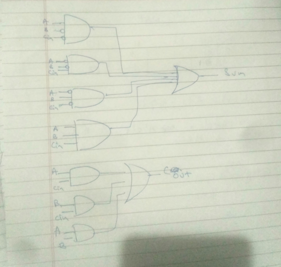
design a 1-bit full adder using a two level OR-AND circuit. Show truth tables, detail logic...
Homework Answers
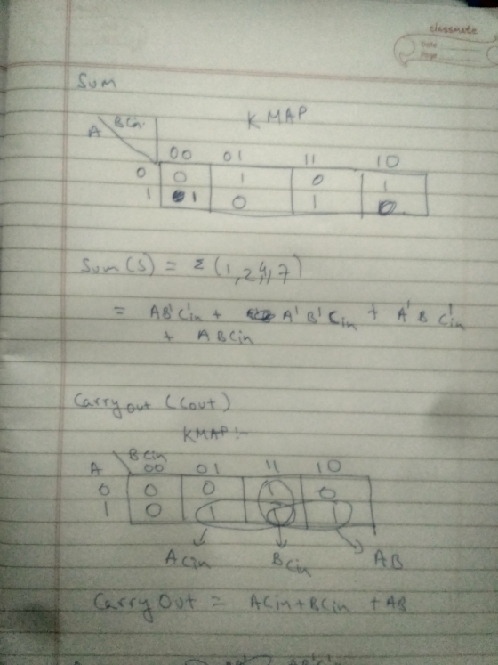
Truth table:-
| A | B | Cin | Cout | Sum |
| 0 | 0 | 0 | 0 | 0 |
| 0 | 0 | 1 | 0 | 1 |
| 0 | 1 | 0 | 0 | 1 |
| 0 | 1 | 1 | 1 | 0 |
| 1 | 0 | 0 | 0 | 1 |
| 1 | 0 | 1 | 1 | 0 |
| 1 | 1 | 0 | 1 | 0 |
| 1 | 1 | 1 | 1 | 1 |
Add Answer to:
design a 1-bit full adder using a two level OR-AND circuit.
Show truth tables, detail logic...
Tim Question 1 Atte 20 pts 2H 24 Design a 1-bit Full Adder using NOR gates...
 Tim Question 1 Atte 20 pts 2H 24 Design a 1-bit Full Adder using NOR gates only, you must include and show: Truth tables, detail logic gate circuit designs, and Boolean expressions Upload Choose a File 20 pts Question 2 Design a 4-bit Full Adder with inputs (Xo...X3, Yo...Y3) in which inputs X are connect to two 4-bit registers via four 2-to-1 Multiplexers and inputs Y are connected to two other 4-bit registers via four 2-to-1 Multiplexers. In this case...
1. A 2-bit adder may be constructed by connection two full adders (i.e. 1-bit adders) or directly...
 Can you please show the work!plzz
1. A 2-bit adder may be constructed by connection two full adders (i.e. 1-bit adders) or directly. For the latter, suppose the inputs (corresponding to the operands A and B) are A, Ao, B1 and Bo; and the outputs are So and S, for the 2-bit sum, S, and a carry-out, C . Give a truth table for the "direct" adder » From the truth table, derive a logic expression in sum-of-products form Give...
Can you please show the work!plzz
1. A 2-bit adder may be constructed by connection two full adders (i.e. 1-bit adders) or directly. For the latter, suppose the inputs (corresponding to the operands A and B) are A, Ao, B1 and Bo; and the outputs are So and S, for the 2-bit sum, S, and a carry-out, C . Give a truth table for the "direct" adder » From the truth table, derive a logic expression in sum-of-products form Give...
5) Following is a NAND only 1-bit full adder circuit diagram. Using this 1-bit full adder...
 5) Following is a NAND only 1-bit full adder circuit diagram. Using this 1-bit full adder a 128-bit combined addition / subtraction circuit (ripple carry implementation) with overflow detection has been implemented using only 2-input NAND logic gate. What is the minimum number of NAND gates required for this circuit? [4pts) CI- Toyota
Verify that your design can be represented by the circuit below. 120 Full-Adder circuit Many of...
 Verify that your design can be represented by the circuit below. 120 Full-Adder circuit Many of the logic gates you require may not exist in standard TTL/CMOS 74 series family of logic. For example in future designs you may require a 50 input OR gate. The 74 series does not have a 50 input OR gate. For your 1 bit adder you will have the following devices: 1 quad 2 IP NAND, 1 TRIPLE 3 IP NAND, 7400 7410 7404...
Design a logic circuit that provides the 2's complement of a 4 bit binary number using...
Design a logic circuit that provides the 2's complement of a 4 bit binary number using adders. Please write the truth table and draw the gate level schematic for it.
by using VIVADO , design 16 bit adder ( code + Testbench) - half adder - full adder using half adder - 4 bit adder using full adder -16 bit adder using 4 bit adder
by using VIVADO , design 16 bit adder ( code + Testbench) - half adder - full adder using half adder - 4 bit adder using full adder -16 bit adder using 4 bit adder
Design a full adder from scratch. (a) Identify inputs and outputs (b) Draw a block diagram...
Design a full adder from scratch. (a) Identify inputs and outputs (b) Draw a block diagram (c) Show the truth tables (d) Determine a minimized Boolean expression for the carry output (e) Draw an AND-OR circuit for the carry output (f) Derive a minimized product-of-sums expression for the carry output of the system
3. PRELAB 1. A half adder is a circuit that has two inputs, A and B,...
 3. PRELAB 1. A half adder is a circuit that has two inputs, A and B, and two outputs, sum and carry. It adds A and B according to the rules of binary addition and outputs the sum and carry. Design a half-adder circuit using one XOR gate and one AND gate. Verify your design through truth table and with Multisim. 2. Whereas the half adder added two inputs A and B, the full adder adds three inputs together, A,...
A full subtractor can be built using two "Half Subtractor" devices and an OR gate. Design...
A full subtractor can be built using two "Half Subtractor" devices and an OR gate. Design and test a full subtractor (schematic diagram and truth table shown below). Write the expressions of the difference and the borrow beside the circuit. Input Output x y bi bi+1 d 0 0 0 0 0 0 0 1 1 1 0 1 0 1 1 0 1 1 1 0 1 0 0 0 1 1 0 1 0 0 1 1 0...
8/8pts Question 1 Using block diagram of 1-bit full adders create a 3-bit parallel adder (show...
 8/8pts Question 1 Using block diagram of 1-bit full adders create a 3-bit parallel adder (show all the connections between the adders and proper outputs Logic Q1jpg 4/9 pts Question 2 Consider your design, if the inputs to be added were 100, and 111, what will be the resulting sum output (Express the resulting sum in binary and base 8 using the least number of bits)? What will be the carry output (Express it only in binary using the least...
 Tim Question 1 Atte 20 pts 2H 24 Design a 1-bit Full Adder using NOR gates only, you must include and show: Truth tables, detail logic gate circuit designs, and Boolean expressions Upload Choose a File 20 pts Question 2 Design a 4-bit Full Adder with inputs (Xo...X3, Yo...Y3) in which inputs X are connect to two 4-bit registers via four 2-to-1 Multiplexers and inputs Y are connected to two other 4-bit registers via four 2-to-1 Multiplexers. In this case...
 Can you please show the work!plzz
1. A 2-bit adder may be constructed by connection two full adders (i.e. 1-bit adders) or directly. For the latter, suppose the inputs (corresponding to the operands A and B) are A, Ao, B1 and Bo; and the outputs are So and S, for the 2-bit sum, S, and a carry-out, C . Give a truth table for the "direct" adder » From the truth table, derive a logic expression in sum-of-products form Give...
Can you please show the work!plzz
1. A 2-bit adder may be constructed by connection two full adders (i.e. 1-bit adders) or directly. For the latter, suppose the inputs (corresponding to the operands A and B) are A, Ao, B1 and Bo; and the outputs are So and S, for the 2-bit sum, S, and a carry-out, C . Give a truth table for the "direct" adder » From the truth table, derive a logic expression in sum-of-products form Give...
 5) Following is a NAND only 1-bit full adder circuit diagram. Using this 1-bit full adder a 128-bit combined addition / subtraction circuit (ripple carry implementation) with overflow detection has been implemented using only 2-input NAND logic gate. What is the minimum number of NAND gates required for this circuit? [4pts) CI- Toyota
 Verify that your design can be represented by the circuit below. 120 Full-Adder circuit Many of the logic gates you require may not exist in standard TTL/CMOS 74 series family of logic. For example in future designs you may require a 50 input OR gate. The 74 series does not have a 50 input OR gate. For your 1 bit adder you will have the following devices: 1 quad 2 IP NAND, 1 TRIPLE 3 IP NAND, 7400 7410 7404...
 3. PRELAB 1. A half adder is a circuit that has two inputs, A and B, and two outputs, sum and carry. It adds A and B according to the rules of binary addition and outputs the sum and carry. Design a half-adder circuit using one XOR gate and one AND gate. Verify your design through truth table and with Multisim. 2. Whereas the half adder added two inputs A and B, the full adder adds three inputs together, A,...
 8/8pts Question 1 Using block diagram of 1-bit full adders create a 3-bit parallel adder (show all the connections between the adders and proper outputs Logic Q1jpg 4/9 pts Question 2 Consider your design, if the inputs to be added were 100, and 111, what will be the resulting sum output (Express the resulting sum in binary and base 8 using the least number of bits)? What will be the carry output (Express it only in binary using the least...
Most questions answered within 3 hours.
-
Where is the error in this code sequence?
String s1 = "Hello";
String s2 = "ello";...
asked 11 months ago -
Financial data for Joel de Paris, Inc., for last year
follow:
Joel de Paris, Inc.
Balance...
asked 11 months ago -
Consider this reaction:
Al2(SO4)3 (aq)+ BaCl3
(aq) Al2Cl6 (aq)- +
3BaSO4(s) . What is the...
asked 11 months ago -
Suppose that Savneet is considering increasing her
recent random sample from 20 car rentals to 40...
asked 11 months ago -
Trucks arrive at an unloading terminal at an average rate of 120
per hour.
Trucks arrive...
asked 11 months ago -
Why are methanol and ethanol completely soluble in water while
octanol is not very little soluble....
asked 11 months ago -
A facilities manager at a university reads in a research report
that the mean amount of...
asked 11 months ago -
When the CuSO4 is rehydrated by adding water to the anhydrous
compound, is this an endothermic...
asked 11 months ago -
A ray of sunlight is passing from diamond into crown glass; the
angle of incidence is...
asked 11 months ago -
A block of mass 0.249 kg is placed on top of a light, vertical
spring of...
asked 11 months ago -
how do the kidneys compensate in the presences of acidosis
a) trigger hyperventilate
b) reserve acid...
asked 11 months ago -
Question 501 pts
The rental rate of capital to the firm increases. Which of the
following...
asked 11 months ago