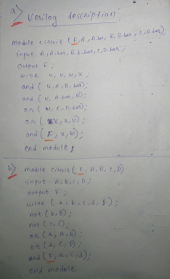
(a) write a Verilog description of the circuit shown below

module Circuit (F, A, A_bar, B, B_bar, C, D_bar); ……….. Endmodule (b) Write a Verilog description of the circuit specified by the following Boolean function:
Z = (A + B’)C’(C + D)
Homework Answers
Add Answer to:
(a) write a Verilog description of the circuit shown below
module Circuit (F, A, A_bar, B,...
HW7.1.1) Which of the Verilog structural descriptions is equivalent to the following Verilog behavioral description? module...
HW7.1.1) Which of the Verilog structural descriptions is equivalent to the following Verilog behavioral description? module hw7_1_1 (x1, x2, x3, f); input x1, x2, x3; output f; assign f = x3 ? x1 : x2; endmodule
HW7.2.3) Which of the Verilog structural descriptions is equivalent to the following Verilog behavioral description? module...
HW7.2.3) Which of the Verilog structural descriptions is equivalent to the following Verilog behavioral description? module hw7_2_3 (x1, x2, x3, f); input x1, x2, x3; output f; always @ (x1, x2, x3) if (x1 == 0) f = x2 & ~x3; else f = ~x2 & x3; endmodule
Draw the circuit corresponding to the Verilog module below. (Do not attempt to simplify the circuit.)...
 Draw the circuit corresponding to the Verilog module below. (Do not attempt to simplify the circuit.) module Circuit A (e, F, G, H); parameter n= 3; input [n-1:0] F, G; input e; output reg [n-1:0] H; integer k; always @ (e, F, G) begin for (k=0; k<n; k=k+1) H[k] = (e | F[k]) & G[k]; end endmodule
Write a test bench to thoroughly test the Verilog module dff_fe_asyn_h. below is the module ddff_fe_asyn_h.code...
Write a test bench to thoroughly test the Verilog module dff_fe_asyn_h. below is the module ddff_fe_asyn_h.code Simulate the circuit using ISim and analyze the resulting waveform. Verilog Code for dff_fe_asyn_h is mentioned below:- //DFF module with asynchronous active high reset with negative edge trigger with clock module dff_fe_asyn_h ( input clock, // Clock Input input reset, // Reset Input input data_in, // Input Data output reg data_out // Output Data ); always @ (negedge clock or posedge reset) // triggers...
Write a test bench to thoroughly test the Verilog module dff_fe_asyn_h. below is the module ddff_fe_asyn_h.code...
Write a test bench to thoroughly test the Verilog module dff_fe_asyn_h. below is the module ddff_fe_asyn_h.code Simulate the circuit using ISim and analyze the resulting waveform. Take full screenshots of all Verilog source codes and the resulting simulation waveform to be included in the lab report. Include explanation of the waveform and how you can conclude that the D flip flop implemented in step 9 is correct in the lab report. Verilog Code for dff_fe_asyn_h is mentioned below:- //DFF module...
why its 4-to-1 mux behavioral? What does the logic circuit represented by the following Verilog module...
 why its 4-to-1 mux behavioral?
What does the logic circuit represented by the following Verilog module do, and what Verilog description style does it use? // My Verilog module #1 module mymodl ( x, d, q) input[1:0] x;input[3:0] d;output q; reg q; wire [1:0] x; wire [3:0] d; always ( x or d) begin case ( x ) 1 : q=d[1]; 2 : g=d[2]; 3 q d[3]; endcase end endmodule
why its 4-to-1 mux behavioral?
What does the logic circuit represented by the following Verilog module do, and what Verilog description style does it use? // My Verilog module #1 module mymodl ( x, d, q) input[1:0] x;input[3:0] d;output q; reg q; wire [1:0] x; wire [3:0] d; always ( x or d) begin case ( x ) 1 : q=d[1]; 2 : g=d[2]; 3 q d[3]; endcase end endmodule
3. (10 Points) RTL Combinational Circuit Design a Draw the schematic for the Verilog code given...
 3. (10 Points) RTL Combinational Circuit Design a Draw the schematic for the Verilog code given below: module abc (a, b, c, d, si, s0); input 31, 30; output a, b, c,d; not (51_, 51), (50_, 0); and (a, s1_, SO_); and (b, s1_, 0); and (c, sl, s0_); and (d, sl, s0); endmodule b. Draw the schematic for the Verilog code given below: module Always_Code input a, b, c, output reg F ); always @(a, b, c) begin F...
Question 3: Realize the circuit below using Verilog. Include a signal “reset_n” for asynchronously clearing the...
 Question 3: Realize the circuit below using Verilog. Include a signal “reset_n” for asynchronously clearing the flip-flop. What type of circuit is this? Complete the following Verilog code. Write a test bench to test it. clk sel module aff (clk, reset_n, sel, q); input clk ; // Declare the inputs and outputs of the module. input reset_n; input sel; output q; reg q; wire D; ; // model the combinational logic assign D= always @( begin if ( else end...
Write a Verilog module that implements the following Boolean equation: f1 = a * b *...
Write a Verilog module that implements the following Boolean equation: f1 = a * b * c' + a * c + b * c Simplify the above expression; write another module to implement it as f2. Write a test bench to check whether f1 and f2 are identical with different values of a, b and c.
Page |3 The function being considered is F(x, y,z)- 20,1,3,4,5,6) 5. Write the Verilog module rep...
 Page |3 The function being considered is F(x, y,z)- 20,1,3,4,5,6) 5. Write the Verilog module representing the minimized function in column I (with primitives). module mod ( outhut
Page |3 The function being considered is F(x, y,z)- 20,1,3,4,5,6) 5. Write the Verilog module representing the minimized function in column I (with primitives). module mod ( outhut
Page |3 The function being considered is F(x, y,z)- 20,1,3,4,5,6) 5. Write the Verilog module representing the minimized function in column I (with primitives). module mod ( outhut
 Draw the circuit corresponding to the Verilog module below. (Do not attempt to simplify the circuit.) module Circuit A (e, F, G, H); parameter n= 3; input [n-1:0] F, G; input e; output reg [n-1:0] H; integer k; always @ (e, F, G) begin for (k=0; k<n; k=k+1) H[k] = (e | F[k]) & G[k]; end endmodule
 why its 4-to-1 mux behavioral?
What does the logic circuit represented by the following Verilog module do, and what Verilog description style does it use? // My Verilog module #1 module mymodl ( x, d, q) input[1:0] x;input[3:0] d;output q; reg q; wire [1:0] x; wire [3:0] d; always ( x or d) begin case ( x ) 1 : q=d[1]; 2 : g=d[2]; 3 q d[3]; endcase end endmodule
why its 4-to-1 mux behavioral?
What does the logic circuit represented by the following Verilog module do, and what Verilog description style does it use? // My Verilog module #1 module mymodl ( x, d, q) input[1:0] x;input[3:0] d;output q; reg q; wire [1:0] x; wire [3:0] d; always ( x or d) begin case ( x ) 1 : q=d[1]; 2 : g=d[2]; 3 q d[3]; endcase end endmodule
 3. (10 Points) RTL Combinational Circuit Design a Draw the schematic for the Verilog code given below: module abc (a, b, c, d, si, s0); input 31, 30; output a, b, c,d; not (51_, 51), (50_, 0); and (a, s1_, SO_); and (b, s1_, 0); and (c, sl, s0_); and (d, sl, s0); endmodule b. Draw the schematic for the Verilog code given below: module Always_Code input a, b, c, output reg F ); always @(a, b, c) begin F...
 Question 3: Realize the circuit below using Verilog. Include a signal “reset_n” for asynchronously clearing the flip-flop. What type of circuit is this? Complete the following Verilog code. Write a test bench to test it. clk sel module aff (clk, reset_n, sel, q); input clk ; // Declare the inputs and outputs of the module. input reset_n; input sel; output q; reg q; wire D; ; // model the combinational logic assign D= always @( begin if ( else end...
 Page |3 The function being considered is F(x, y,z)- 20,1,3,4,5,6) 5. Write the Verilog module representing the minimized function in column I (with primitives). module mod ( outhut
Page |3 The function being considered is F(x, y,z)- 20,1,3,4,5,6) 5. Write the Verilog module representing the minimized function in column I (with primitives). module mod ( outhut
Page |3 The function being considered is F(x, y,z)- 20,1,3,4,5,6) 5. Write the Verilog module representing the minimized function in column I (with primitives). module mod ( outhut
Most questions answered within 3 hours.
-
Where is the error in this code sequence?
String s1 = "Hello";
String s2 = "ello";...
asked 11 months ago -
Financial data for Joel de Paris, Inc., for last year
follow:
Joel de Paris, Inc.
Balance...
asked 11 months ago -
Consider this reaction:
Al2(SO4)3 (aq)+ BaCl3
(aq) Al2Cl6 (aq)- +
3BaSO4(s) . What is the...
asked 11 months ago -
Suppose that Savneet is considering increasing her
recent random sample from 20 car rentals to 40...
asked 11 months ago -
Trucks arrive at an unloading terminal at an average rate of 120
per hour.
Trucks arrive...
asked 11 months ago -
Why are methanol and ethanol completely soluble in water while
octanol is not very little soluble....
asked 11 months ago -
A facilities manager at a university reads in a research report
that the mean amount of...
asked 11 months ago -
When the CuSO4 is rehydrated by adding water to the anhydrous
compound, is this an endothermic...
asked 11 months ago -
A ray of sunlight is passing from diamond into crown glass; the
angle of incidence is...
asked 11 months ago -
A block of mass 0.249 kg is placed on top of a light, vertical
spring of...
asked 11 months ago -
how do the kidneys compensate in the presences of acidosis
a) trigger hyperventilate
b) reserve acid...
asked 11 months ago -
Question 501 pts
The rental rate of capital to the firm increases. Which of the
following...
asked 11 months ago